If you have a related question, please click the "Ask a related question" button in the top right corner. The newly created question will be automatically linked to this question.
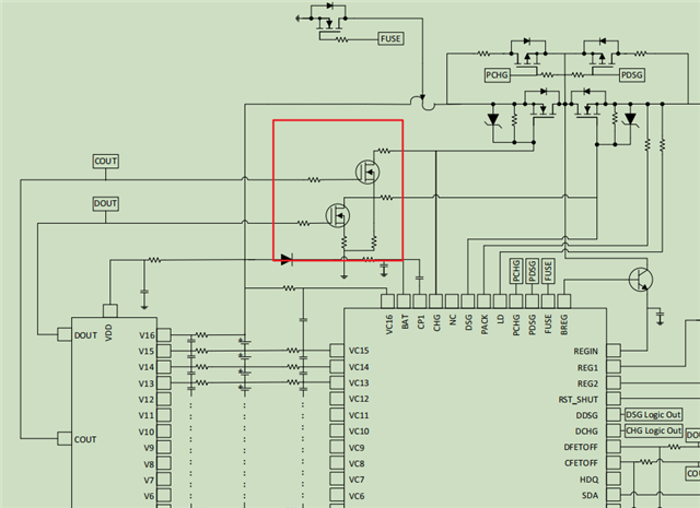
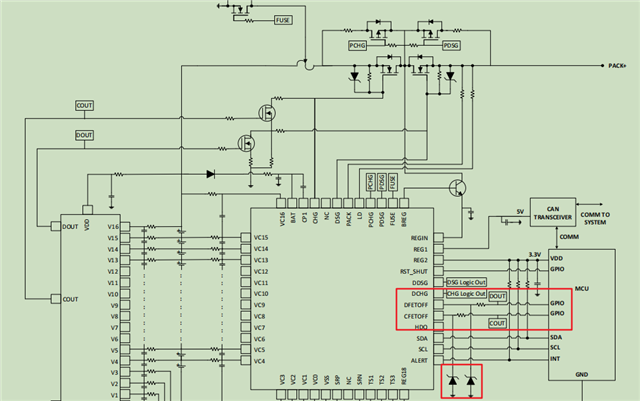
您好,this configuration pulls down the CHG gate to GND. This is why the image you shared also shows DOUT and COUT being connected to DFETOFF and CFETOFF respectively. This ensures that the BQ779216 turns off the FET drivers of the BQ76952 and avoid discharging the charge-pump.
The pull-down resistance must be chosen to not draw too much current from the battery.
If they wanted to pull down the gate without using the DFETOFF/CFETOFF pins, then they would likely need additional circuitry to ensure the BQ76952 charge pump does not become discharged.
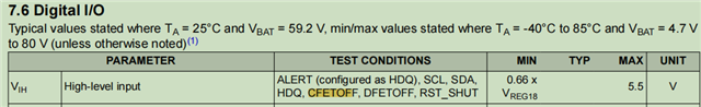
您好,You are correct that the recommended max for CFETOFF is 5.5-V. I've seen customers use 5-V or 5.5-V Zeners in order to limit the voltage into the pins. The figure is an example, it does not necessarily need to connect to the MCU.
They could simply connect the same clamped voltage into the BQ76952 and the MCU through the same line.