This thread has been locked.
If you have a related question, please click the "Ask a related question" button in the top right corner. The newly created question will be automatically linked to this question.
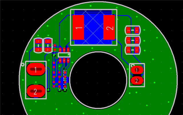
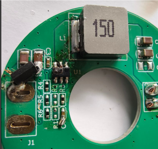
这是PCB板Layout 图,请帮分析下原因,感谢!
感谢您对TI产品的关注!关于你的咨询,你的设计电流是多大的,电感选择是否合理。注意功率电感饱和电流足够大。
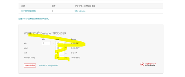
你用芯片主页的webench工具导出设计,仿一下看看。
https://www.ti.com.cn/product/cn/TPS56339
GND多打一些过孔,电流泄放会快一些。
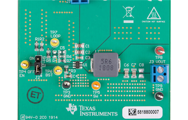
评估板设计例。
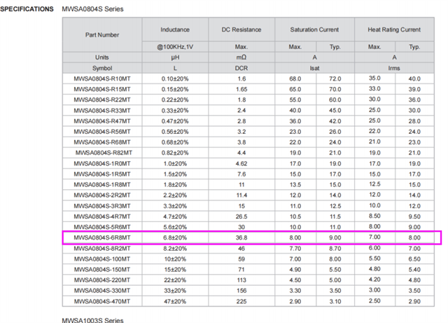
您好!非常感谢您及时回复,功率电感参数如下,这边发现在不带负载情况下,平凡插拔输入电源,这种情况下比较容易出现烧芯片情况,会是什么原因呢,有方法解决这种问题吗?感谢
突入电流或突入电压过大,你看看输入端加一个小的阻值的防浪涌的电阻看看是否有改善。
电感参数,你可以看看webench导出的电路中推荐的电感型号跟电感参数。
上面提示你了,芯片主页的设计开发中有webench工具,输入你的设计参数,会自动生成电路。
好的,这边尝试下,感谢!
当出问题后输入端也尝试加肖特基2级管,也会烧芯片现象,等换了电感在尝试试,谢谢!
好的,客气了。
您好!
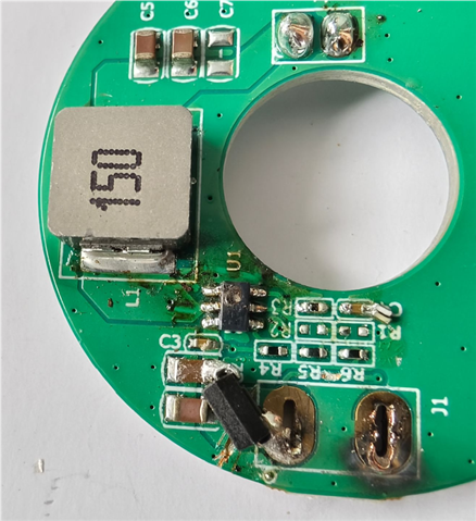
按照您提的建议,更换了电感值,测试还是一样会烧芯片,以上是图片,您帮再分析下还有可能是哪有问题呢,感谢!
一般都是电流电压过大,或ESD才造成芯片损毁, 你的PCB板还有短路的地方吗?
测量过吗
您好!感谢您及时回复,这电流是指输入电流?电压是输入24VDC,但输入电压低压20VDC以下,就不会有这问题,PCB在接电前一定是没有短路的地方,都有测量过,这种损坏芯片在不带负载情况下都会损坏芯片。ESD是指瞬间接入产生的吗?如果是瞬间接入引起,您这边是否有好的解决方案。感谢!
ESD对策的话,是输入端加TVS,齐纳二极管或肖特基二极管,抑制瞬态电压。
但看你的描述,电压是输入24VDC,但输入电压低压20VDC以下,就不会有这问题,那你是输入端超过芯片最大定格电压了。
你测量下是否超过芯片最大定格了。
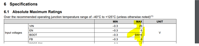
感谢您回复,VIN电压一定不会超过24VDC,EN用芯片内部没外部加控制,BOOT以及FB都是官方提供的参数来的,排除这些因素外,还有其他防范措施吗?感谢!
其他的原因就不清楚了,但从你的描述。
超出芯片最大定格的可能性较大,最好在详细测量下。
感谢您的回复,这些基本条件是一定在标准范围内,也都测量过。
那你输入端加ESD保护看看有没有改善