This thread has been locked.

If you have a related question, please click the "Ask a related question" button in the top right corner. The newly created question will be automatically linked to this question.

LM3481: when the low temperature , the power supply can't start when the EN signal occur

Part Number: LM3481


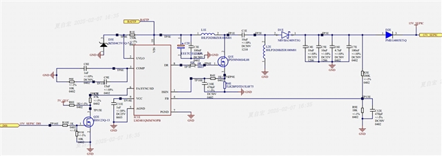
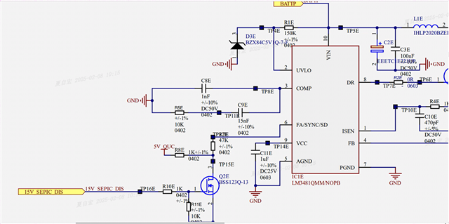
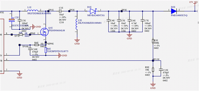
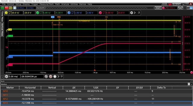
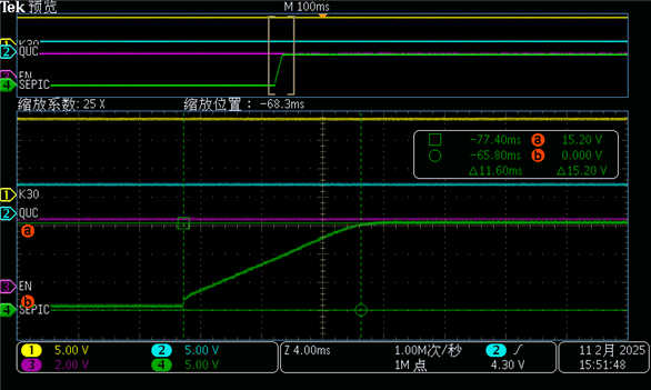
 We use the IC for SEPIC for inverter‘s resolver‘s power, when the temp=-20℃ on vehicle ,at the start time,the fault UV occur ,the sepic output can't output voltage。

But when other High and low temperature testing,the sepic is working good。

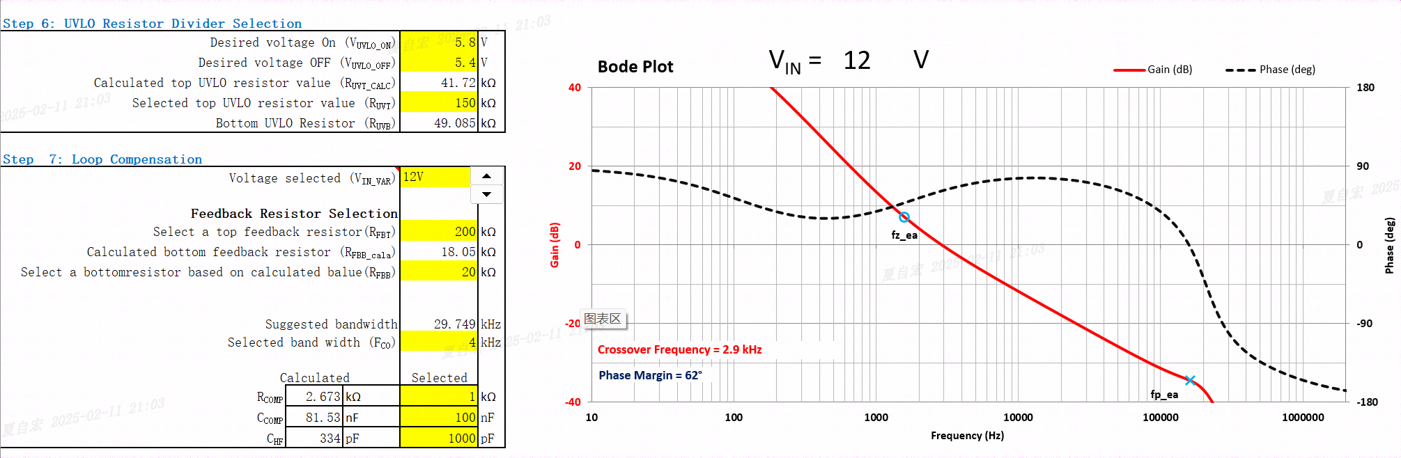
Please help me check the peripheral circuit parameter about the LM3481, and if the stability of the loop is ok,thanks.

LM3481 PARAMETER 

  • For a schematic review, can you re-attach the file in higher quality? I cannot read the component values.
    Can you also give be VIN, VOUT target and maximum load current?

  • Thank you for your repply, the upper SCH picture is the higher quality picture.

    and for target , the Vin=6~24V, Vout=15.4V@±1%,

    the rated load is 0.15A, and we design the maximum  load current is 0.45A(Reserve for three times the rated load),  but in usually, we provide current to the  resolver transformer at 0.085A.

    That's the parameter, thank you very much~

  • The compensation is quite aggressive. I would recommend to choose a slower compensation to make the system more stable.
    Example values:
    R5E: 10kOhm --> 1kOhm
    C9E: 15nF --> 100nF

    Afterwards they can run a test to see if the behavior improves at low temperature.
    If the issue does not solve, it would be helpful if they could send waveform measurements of VOUT together with the Switch Node signal (TP1E) during stable and unstable behavior.

  • Thank you for your repply, I have change the  values:

    R5E: 10kOhm --> 1kOhm
    C9E: 15nF --> 100nF

    and the 0% load to 100% load 150mA start time from 14.2ms change to 12.4ms; the picture is below: The CH4: red line to CH4: green line.

    how can we evaluate whether the slope compensation parameters are reasonable ?

    The follow picture is the calculate  excel file I have download from ti official website.

    And by the way, what's the suitbale crossover frequncy and phase margin? I see the AN 1286 said, the crossover frequency is 2KHz with a phase margin of 60 degrees is suitble, can you give me some suggestion? thank you

  • Thanks for the update.
    The waveforms look stable to me.

    For designing the compensation, we recommend a phase margin of 60 degree more more to avoid risks of oscillation or strong overshoots under worst case conditions.
    For crossover frequency, higher values will create a faster loop reaction, hence smaller overshoots when a transient occurs.
    However, higher crossover frequency can come at the cost of smaller phase margin. This depends on the design and compensation.
    To give a reference based on experience, 1kHz - 20kHz is a common crossover frequency range for such SEPIC converter designs.

    There is a lot of theory that goes into more detail on this.
    An example is given here:
    https://www.ti.com/lit/an/slva381b/slva381b.pdf