

When we talk about mos, most people are familiar with the term.
The "N" in Nmos comes from the word Negative, indicating that the primary charge carriers involved in conduction are negatively charged electrons in this type of semiconductor.
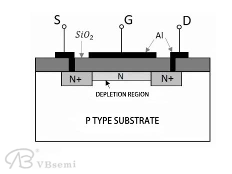
nmos is a form of mos that uses N-type semiconductor material as the conductive channel.
The Birth of mos:
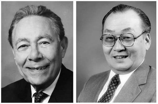
In 1962, Dawon Kahng and Martin Atalla from Bell Labs in the United States successfully developed the Metal-Oxide-Semiconductor Field-Effect Transistor (mosFET). This invention became a major milestone in the history of semiconductor development, and they are often referred to as the "fathers" of the mosFET.
Early Characteristics and Limitations of Nmos:
Early Nmos technology, with its significant advantages, largely replaced BJT (Bipolar Junction Transistor) in many applications.
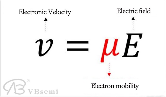
1.Higher Switching Speed: Nmos has a higher electron mobility compared to Pmos, meaning electrons move faster in Nmos, and thus Nmos circuits can switch faster.
2.Lower Static Power Consumption: Unlike traditional circuits, Nmos only allows current to flow during switching operations, so it has lower static power consumption in comparison.
Despite its advantages, early Nmos also faced several limitations due to the technology of the time:
1.Higher Dynamic Power Consumption: Early Nmos circuits consumed significant dynamic power during switching, especially when frequently toggling. The charge injection and capacitor discharge during switching led to higher power dissipation.
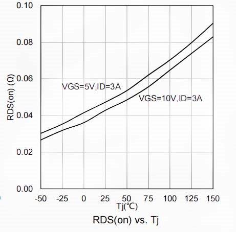
2.Temperature Sensitivity: Nmos circuits were quite sensitive to temperature variations. As temperature increased, the resistance of Nmos devices rose, leading to a decline in performance and potentially affecting circuit stability.
However, technology continued to evolve, and semiconductor advancements led to innovations in Nmos.
Modern Nmos devices are integrated into billions of transistors in processors and memory chips. Thanks to advanced photolithography techniques, Nmos devices are now mass-produced on a large scale.
In the ongoing pursuit of technological advancements, every turning point brings a revolutionary change, reshaping our understanding of the world.
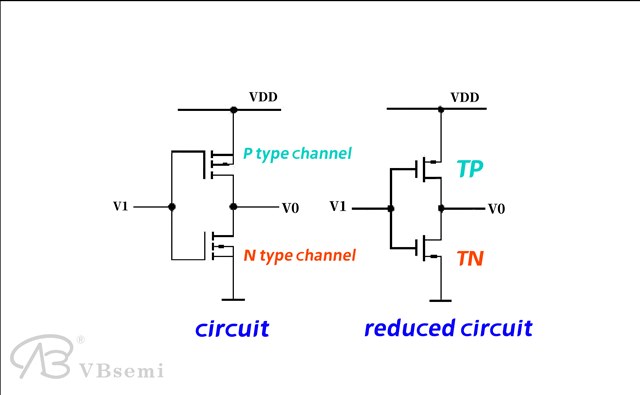
In the 1980s, Nmos reached another transformative milestone with the introduction of Cmos (Complementary Metal-Oxide-Semiconductor) technology, which became the dominant technology in integrated circuits.
Cmos combines the strengths of both Nmos and Pmos, utilizing complementary working principles to achieve low power consumption, high speed, and high integration.
This innovation was a brilliant response to traditional challenges in semiconductor technology, allowing for better efficiency and greater versatility. Cmos technology has continued to expand its applications and is now the driving force behind the development and innovation of modern electronic products.
From the early days of single Nmos transistors to today's widespread use of Cmos technology, Nmos has undergone decades of development and innovation. Its applications have steadily penetrated our daily lives, often without us even noticing.
In the future, the continued innovation in Nmos will shape our lives and unlock unprecedented possibilities.


