我使用的代码是pdk下面的ddr3 初始化例程,发现不管我是否启动leveling,或启动后是否进行延时等待,0x21000004的leveling状态寄存器始终都是0x40000004的值,这个值表示leveling未超时,且IFRDY bit为1表示leveling 完成;
这个现象让我怀疑leveling是否有进行,我的问题是:
1、我该如何查看通过Full Automatic Leveling的参数结果?
2、我该如何确认Full Automatic Leveling是否已经完成?
void ddr3_setup_auto_lvl_1333()
{
//int i,TEMP,startlo, stoplo,starthi, stophi;
int TEMP;
KICK0 = KICK0_UNLOCK;
KICK1 = KICK1_UNLOCK;
/* Wait for PLL to lock = min 500 ref clock cycles.
With refclk = 100MHz, = 5000 ns = 5us */
sleep_timer(1000);
/***************** 3.2 DDR3 PLL Configuration ************/
/* Done before */
/**************** 3.0 Leveling Register Configuration ********************/
/* Using partial automatic leveling due to errata */
/**************** 3.3 Leveling register configuration ********************/
DDR3_CONFIG_REG_0 &= ~(0x007FE000); // clear ctrl_slave_ratio field
DDR3_CONFIG_REG_0 |= 0x00200000; // set ctrl_slave_ratio to 0x100
DDR3_CONFIG_REG_12 |= 0x08000000; // Set invert_clkout = 1
DDR3_CONFIG_REG_0 |= 0xF; // set dll_lock_diff to 15
//From 4.2.1 Executing Partial Automatic Leveling -- Start
DDR3_CONFIG_REG_23 |= 0x00000200; //Set bit 9 = 1 to use forced ratio leveling for read DQS
//From 4.2.1 Executing Partial Automatic Leveling -- End
//Values with invertclkout = 1
/**************** 3.3 Partial Automatic Leveling ********************/
/*DATA0_WRLVL_INIT_RATIO = 0x78;
DATA1_WRLVL_INIT_RATIO = 0x76;
DATA2_WRLVL_INIT_RATIO = 0x72;
DATA3_WRLVL_INIT_RATIO = 0x76;
DATA4_WRLVL_INIT_RATIO = 0x69;
DATA5_WRLVL_INIT_RATIO = 0x69;
DATA6_WRLVL_INIT_RATIO = 0x5B;
DATA7_WRLVL_INIT_RATIO = 0x60;
DATA8_WRLVL_INIT_RATIO = 0x00;
DATA0_GTLVL_INIT_RATIO = 0xAF;
DATA1_GTLVL_INIT_RATIO = 0xB1;
DATA2_GTLVL_INIT_RATIO = 0xA3;
DATA3_GTLVL_INIT_RATIO = 0xA0;
DATA4_GTLVL_INIT_RATIO = 0x9B;
DATA5_GTLVL_INIT_RATIO = 0x9B;
DATA6_GTLVL_INIT_RATIO = 0x98;
DATA7_GTLVL_INIT_RATIO = 0x92;
DATA8_GTLVL_INIT_RATIO = 0x00; */
//Do a PHY reset. Toggle DDR_PHY_CTRL_1 bit 15 0->1->0
DDR_DDRPHYC &= ~(0x00008000);
DDR_DDRPHYC |= (0x00008000);
DDR_DDRPHYC &= ~(0x00008000);
/***************** 3.4 Basic Controller and DRAM Configuration ************/
DDR_SDRFC = 0x0000c34; // enable configuration
/* DDR_SDTIM1 = 0x1113783C; */
TEMP = 0;
TEMP |= 0x8 << 25; // T_RP bit field 28:25
TEMP |= 0x8 << 21; // T_RCD bit field 24:21
TEMP |= 0x9 << 17; // T_WR bit field 20:17
TEMP |= 0x17 << 12; // T_RAS bit field 16:12
TEMP |= 0x20 << 6; // T_RC bit field 11:6
TEMP |= 0x7 << 3; // T_RRD bit field 5:3
TEMP |= 0x4; // T_WTR bit field 2:0
DDR_SDTIM1 = 0x0AAAE4E2; //TEMP;
/* DDR_SDTIM2 = 0x30717FE3; */
TEMP = 0;
TEMP |= 0x3 << 28; // T_XP bit field 30:28
TEMP |= 0x71 << 16; // T_XSNR bit field 24:16
TEMP |= 0x1ff << 6; // T_XSRD bit field 15:6
TEMP |= 0x4 << 3; // T_RTP bit field 5:3
TEMP |= 0x3; // T_CKE bit field 2:0
DDR_SDTIM2 = 0x206B7FDA;//TEMP;
/* DDR_SDTIM3 = 0x559F86AF; */
TEMP = 0;
TEMP |= 0x5 << 28; // T_PDLL_UL bit field 31:28 (fixed value)
TEMP |= 0x5 << 24; // T_CSTA bit field 27:24 (fixed value)
TEMP |= 0x4 << 21; // T_CKESR bit field 23:21
TEMP |= 0x3f << 15; // T_ZQCS bit field 20:15
TEMP |= 0x6a << 4; // T_RFC bit field 12:4
TEMP |= 0xf; // T_RAS_MAX bit field 3:0 (fixed value)
DDR_SDTIM3 = 0x557F867F; //TEMP;
DDR_DDRPHYC = 0x0010010F;
DDR_ZQCFG = 0x70073214;
DDR_PMCTL = 0x0;
DDR_SDRFC = 0x0000c34; // enable configuration
/* DDR_SDCFG = 0x63062A32; */
/* New value with DYN_ODT disabled and SDRAM_DRIVE = RZQ/7 //0x63222A32; // last config write DRAM init occurs */
TEMP = 0;
TEMP |= 0x3 << 29; // SDRAM_TYPE bit field 31:29 (fixed value)
TEMP |= 0x0 << 27; // IBANK_POS bit field 28:27
TEMP |= 0x3 << 24; // DDR_TERM bit field 26:24
TEMP |= 0x0 << 21; // DYN_ODT bit field 22:21
TEMP |= 0x1 << 18; // SDRAM_DRIVE bit field 19:18
TEMP |= 0x2 << 16; // CWL bit field 17:16
TEMP |= 0x0 << 14; // NM bit field 15:14
TEMP |= 0xA << 10; // CL bit field 13:10
TEMP |= 0x4 << 7; // ROWSIZE bit field 9:7
TEMP |= 0x3 << 4; // IBANK bit field 6:4
TEMP |= 0x0 << 3; // EBANK bit field 3:3
TEMP |= 0x2; // PAGESIZE bit field 2:0
DDR_SDCFG = 0x63072B33;//TEMP;
//Wait 600us for HW init to complete
sleep_timer(100000);
DDR_SDRFC = 0x0000c34; //0x00001450; //Refresh rate = (7.8*666MHz)
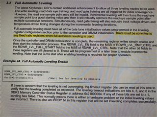
/**************** 4.2.1 Executing Partial Automatic Leveling ********************/ 重要问题::执行此部分后,我如何查看通过leveling之后得到的RATIO参数结果?
DDR_RDWR_LVL_RMP_CTRL = 0x80000000; //enable full leveling
DDR_RDWR_LVL_CTRL = 0x80000000; //Trigger full leveling - This ignores read DQS leveling result and uses ratio forced value
//(0x34) instead
//Wait for min 1048576 DDR clock cycles for leveling to complete = 1048576 * 1.5ns = 1572864ns = 1.57ms.
//Actual time = ~10-15 ms
sleep_timer(100000);
//GEL_TextOut("\nDDR3 initialization is complete.\n");
}
附上手册中对Full leveling的描述:问题2: 说IFRDY bit用来指示 leveling complete successfully,但似乎这一bit,不管是否启动leveling,始终都为1?