This thread has been locked.

If you have a related question, please click the "Ask a related question" button in the top right corner. The newly created question will be automatically linked to this question.

AWRL6432: Some questions about AWRL6432 memory and EDMA

Part Number: AWRL6432

Hello,

I have the following questions that I would like answered:

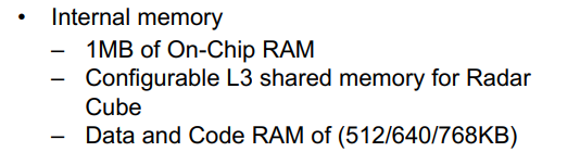
1. Generally speaking, when the chip is booted, the code and data of the external flash will be loaded into the code ram and data ram of the chip. In this chip, is there a concept of code ram and data ram? which is the corresponding memory?

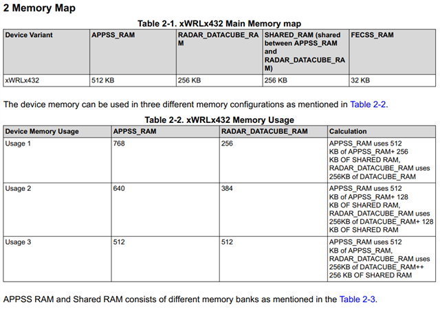
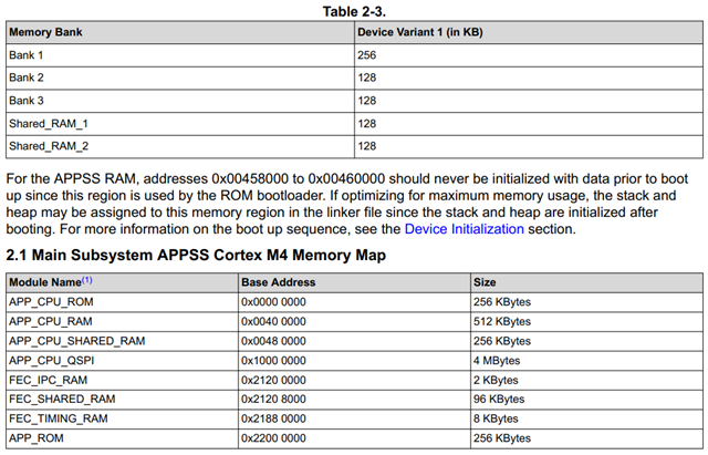
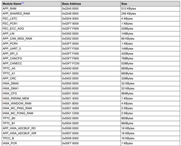
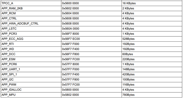
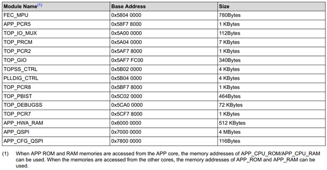
2. In the document AWRL6432 reference manual, Section 2.1,Main Subsystem APPSS Cortex M4 Memory Map, Is there any more detailed information to explain this?

3. What memory addresses can EDMA access? I tried, but the address 0x00400000 is not accessible by EDMA, but 0x22400000 is.

Looking forward to hearing from you.

  • Code RAM and Data RAM:
    Many microcontrollers or processors have separate regions for code (instructions) and data in their memory maps. The code typically resides in Flash memory, and during booting, it might be copied to RAM for faster execution. Data, on the other hand, is often stored in different RAM regions.


    EDMA Accessible Memory Addresses:
    EDMA controllers are configured to transfer data between specific source and destination addresses. The accessible addresses depend on the configuration of the EDMA controller and the memory map of the device. The fact that you can access 0x22400000 but not 0x00400000 might be related to the specific memory configuration or protection settings.

  • Hello Gary,

    Do you have more detailed information about memory?

  • For your reference, here are more detailed instructions:www.ti.com.cn/.../swru599.pdf

  • Hi Gary,

    Thanks for your response.

    I do have the reference documentation, but in Chapter 2, the Memory Map, I can only see a brief description of the memory, but no more detailed description information.

    Let me describe some of the problems in more detail:

    1. In  2.1 Main Subsystem APPSS Cortex M4 Memory Map,   APP_CPU_ROM, APP_CPU_RAM, APP_CPU_SHARED_RAM, APP_RAM, APP_SHARED_RAM, APP_ROM, APP_HWA_RAM, etc., what are the roles of these memory, and what are the differences?

    2. The ram size of the chip 6432 is 1MBytes. According to Table 2-1, it consists of APPSS_RAM, RADAR_DATACUBE_RAM, and SHARED_RAM. Which memory region does APPSS_RAM, RADAR_DATACUBE_RAM, SHARE_RAM correspond to?

    3. Which memory areas can EDMA access? Where can I find out from the documentation?

  • Hello,

    APP_CPU_ROM`: This is read-only memory for the application code running on the Cortex-M4 CPU.
    APP_CPU_RAM`: This is the random-access memory for the Cortex-M4 CPU to store data during runtime.
    APP_CPU_SHARED_RAM`: Shared memory accessible by both the Cortex-M4 CPU and other parts of the system.
    APP_RAM`:General RAM for the application.
    APP_SHARED_RAM`: Shared RAM for the application.
    APP_ROM`: ROM for the application.
    APP_HWA_RAM`: RAM for the hardware accelerator.
    APPSS_RAM`:This is the RAM dedicated to the application subsystem.
    RADAR_DATACUBE_RAM`: RAM dedicated to radar data cube processing.
    SHARED_RAM`: Shared RAM accessible by multiple components.

  • Hi,

    I have some understanding: APP_CPU_RAM, ROM, SHARED_RAM can only be accessed by the CPU, except for the CPU, other can not be accessed, is this understanding correct?

    Also, what does APP_RAM, ROM, SHARED_RAM have to do with APP_CPU_RAM, ROM, SHARED_RAM? Is the APP's memory loaded into the APP_CPU during initialization? If both can be used at the same time, then why does the manual mention that APPSS_RAM size is 512KB? APP_RAM + APP_CPU_RAM = 1024KB

  • Hello,

    Your understanding is correct

    "APP_CPU_RAM," ROM, and "SHARED_RAM" are usually accessible by the CPU, with other components having restricted access.

    In terms of the relationship between "APP_RAM," ROM, and "SHARED_RAM" with "APP_CPU_RAM," ROM, and "SHARED_RAM," these terms likely refer to different memory regions used by the application and other system components.

    As for the manual's mention of "APPSS_RAM" size being 512KB and the sum of "APP_RAM" and "APP_CPU_RAM" being 1024KB, this likely reflects the specific memory layout and allocation for the application and CPU within the system. The manual may be highlighting these sizes to provide clarity on the available memory resources for different components.

    Regards,

    Gary

  • Hello Gary,

    In AWRL6432 datasheet - Chapter 1. Features - Internal memory, 

    In AWRL6432 reference manual - Chapter 2 - Memory Map,

    What memory does 1MB of On-Chip RAM contain that is mentioned in the RM documentation?

    And Configurable L3 shared memory for Radar Cube、 Data and Code RAM of (512/640/768KB)?

  • Hello,

    In the AWRL6432 datasheet and reference manual, the 1MB of On-Chip RAM likely refers to the total amount of random access memory (RAM) available on the chip for various purposes such as data storage, program execution, and other system operations.

    The Configurable L3 shared memory for Radar Cube, Data, and Code RAM (512/640/768KB) likely refers to a specific portion of the on-chip RAM that can be allocated and configured for different purposes, such as storing radar data, code, and other data. The specific allocation size (512/640/768KB) may indicate the flexibility in how this shared memory can be partitioned for different functions.

    Regards,

    Gary