Part Number: OPA860
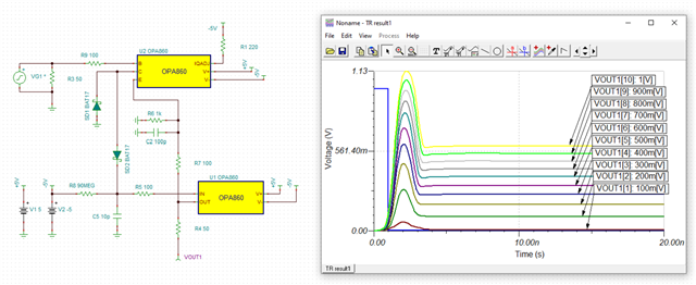
Recently I am working on the peak sampling circuit of OPA860. I used the reference circuit provided by TI engineers. TINA simulation can be used. Under the same configuration, when the input in LTSPICE is zero, the peak hold output has a bias voltage of 100mV. The made PCB The function cannot be realized, and the circuit is sure that there are no other electrical errors. The signal input of the board is zero, the input side of the SD2 diode is -0.4V, the output side of the SD2 diode is nearly 4V, and the board outputs 3.8V. Moreover, no matter how the input changes, the output is always 3.85V. Ask an engineer how to solve this problem? thanks