Part Number: LMX2820
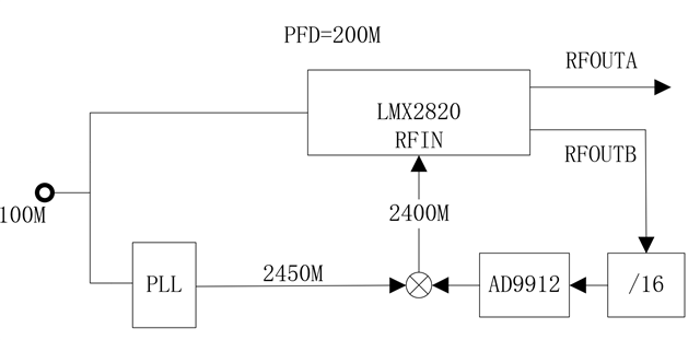
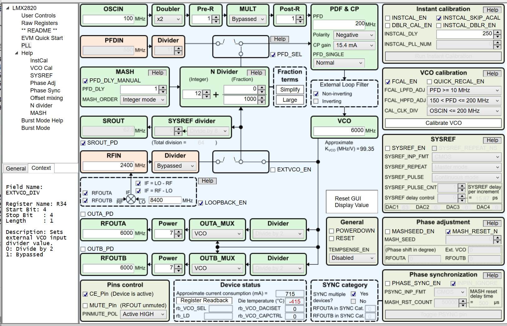
the above is my schematic diagram,i use loopback mode,and the registers configuration is as following,but i can't lock,how to configure the register
mem[0] <= 24'h4F001E ; //R79 [8] OUTB_PD 0:normal 1:pwr down ;[5:4]OUTB_MUX 0 = Channel divider,1=VCO,2=VCO doubler ;[3:1] OUTA_PWR
mem[1] <= 24'h4E0001 ; //R78 [4]OUTA_PD [1-0]OUTA_MUX
mem[2] <= 24'h4D0608 ; //R77 [7] PINMUTE_POL Sets the polarity of mute control for MUTE pin. 0x0 = Active HIG 0x1 = Active LOW
mem[3] <= 24'h46000E ; //R70 [7]DBLBUF_OUTMUX_EN [6]DBLBUF_OUTBUF_EN [5]DBLBUF_CHDIV_EN [4]DBLBUF_PLL_EN
mem[4] <= 24'h440020 ; //R68
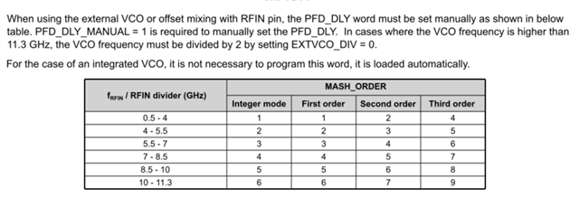
mem[5] <= 24'h250300 ; //R37 PFD_DLY
mem[6] <= 24'h24000C ; //R36 [14:0] PLL_N Sets N divider value
mem[7] <= 24'h233000 ; //R35 [8:7] MASH_ORDER 0=Integer mode
mem[8] <= 24'h220810 ; //R34 LOOPBACK_EN=1 EXTVCO_DIV=1
mem[9] <= 24'h171103 ; //R23 [0] VCO_SEL_FORCE 0x0 = Disable 0x1 = Enabled Forces the VCO to use the core specified by VCO_SEL Useful for full-assisted VCO calibration and debugging purposes.
mem[10] <= 24'h1622BF ; //R22 [15:13]VCO_SEL [7:0]VCO_CAPCTRL VCO1 5.65~6.35G VCO2 6.35~7.3G VCO3 7.3~8.1G
mem[11] <= 24'h120000 ; //R18
mem[12] <= 24'h1115C0 ; //R17
mem[13] <= 24'h10171E ; //R16 [4:1] CPG
mem[14] <= 24'h0F2001 ; //R15 [11] PFD_POL [10:9]PFD_SINGLE 0x0 = Normal operation 0x3 = Single PFD
mem[15] <= 24'h0D0038 ; //R13 [12:5]PLL_R Sets reference path Post-R divider value.
mem[16] <= 24'h0B0612 ; //R11 [4] OSC_2X 0 = Disabled 1=enable
mem[17] <= 24'h0A1000 ; //R10 [12]PFD_DLY_MANUAL
mem[18] <= 24'h070000 ; //R7
mem[19] <= 24'h050032 ; //R5
mem[20] <= 24'h030041 ; //R3
mem[21] <= 24'h0281F4 ; //R2 [14:12]CAL_CLK_DIV [11:1] INSTCAL_DLY [0]QUICK_RECAL_EN
mem[22] <= 24'h0157A0 ; //R1
mem[23] <= 24'h006430 ; //R0