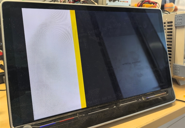
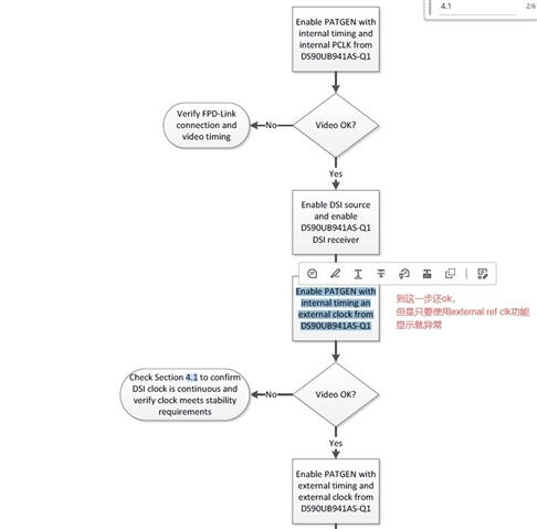
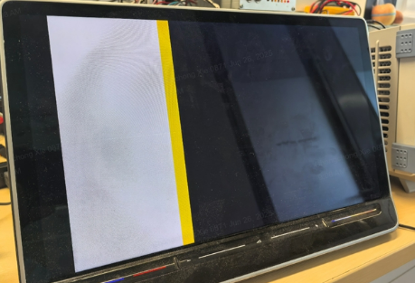
We want to try to use External Reference Clock Mode mode to light up the display on the DS90UB941 (the Ref Clk clock source comes from OUTPUT0 of the LMK3H0102-Q1 chip). What registers do we need to configure? The External DSI Clock and Ext timing we are currently using. I tried to add 0x56 to write 0x01 based on the following configuration. I don’t know if the configuration timing is incorrect, so the screen is black.
119 static struct dsi_panel_param dsi_panel_parameter[] = { 120 //15inch 121 { 122 .t_clk_post = 0x0e, 123 .t_clk_pre = 0x1e, 124 .h_active = 2240, 125 .v_active = 1260, 126 .h_front_porch = 24, 127 .h_back_porch = 40, 128 .h_sync_width = 28, 129 .v_front_porch = 6, 130 .v_back_porch = 4, 131 .v_sync_width = 2, 132 },
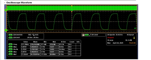
dsi clock = v total * h total * fps = (1260+6+4+2) * (2240+24+40+28) * 60 = 177,978,240 HZ
Our current DS90UB941 configuration is as follows. How to add the ref clk mode on this basis
writeLvdsRegister(0x01,0x08);
writeLvdsRegister(0x40,0x04);
writeLvdsRegister(0x41,0x05);
writeLvdsRegister(0x42,0x3C); //DPHY_SKIP_TIMING
writeLvdsRegister(0x41,0x21); //DSI_CONFIG_1
//DSI_VS_POLARITY:1->VS signal is active low;DSI_HS_POLARITY:1->HS signal is active low;DSI_NO_EOTPKT:1
writeLvdsRegister(0x42,(1<<6)|(1<<5)|(1<<0));
writeLvdsRegister(0x01,0x00);
您好,
请参考DS90UB941AS-Q1 DSI Bringup Guide
请使用“"Figure 3-2. Recommended DS90UB941AS-Q1 Bring-Up Flow" ”配置,并使用PatGen进行测试验证。
请注意DSI clock frequency = ((pixel clock rate) * bits per pixel) / (2 * number of DSI lanes)
下面脚本请参考
## Pixel Clock = 148.5 MHz (eg. for standard 1080p) ## DSI clock = 445.5 MHz ## DSI input port 0 ## 4 lanes DSI import time serAddr = 0x18 desAddr0 = 0x58 #RESET 941 board.WriteI2C(serAddr,0x01,0x02) #Disable DSI board.WriteI2C(serAddr,0x01,0x08) board.WriteI2C(serAddr,0x1E,0x01) # Select DSI0 board.WriteI2C(serAddr,0x4F,0x8C) # Set single DSI0 mode - continuous clock mode board.WriteI2C(serAddr,0x40,0x04) # TSKIP_CNT DSI0 board.WriteI2C(serAddr,0x41,0x05) # TSKIP_CNT DSI0 board.WriteI2C(serAddr,0x42,0x30) # TSKIP_CNT DSI0, TSKIP_CNT (dec)= 24 board.WriteI2C(serAddr,0x40,0x04) # Set HSYNC/VSYNC Polarity DSI0 board.WriteI2C(serAddr,0x41,0x21) # Set HSYNC/VSYNC Polarity DSI0 board.WriteI2C(serAddr,0x42,0x60) # Set HSYNC/VSYNC Polarity DSI0 board.WriteI2C(serAddr,0x40,0x10) # Init DSI Clock Settings (From Section 10.2 of datasheet) board.WriteI2C(serAddr,0x41,0x86) # Init DSI Clock Settings (From Section 10.2 of datasheet) board.WriteI2C(serAddr,0x42,0x0A) # Init DSI Clock Settings (From Section 10.2 of datasheet) board.WriteI2C(serAddr,0x41,0x94) # Init DSI Clock Settings (From Section 10.2 of datasheet) board.WriteI2C(serAddr,0x42,0x0A) # Init DSI Clock Settings (From Section 10.2 of datasheet) #Enable DSI board.WriteI2C(serAddr,0x01,0x00)
Hello TI:
如下是我们的配置,使用的external ref clk和internal timing,验证下来黑屏,如果去掉external ref clk则显示彩虹条
writeLvdsRegister(0x01,0x08);
writeLvdsRegister(0x40,0x04);
writeLvdsRegister(0x41,0x05);
writeLvdsRegister(0x42,0x3c); //DPHY_SKIP_TIMING
writeLvdsRegister(0x41,0x21); //DSI_CONFIG_1
//DSI_VS_POLARITY:1->VS signal is active low;DSI_HS_POLARITY:1->HS signal is active low;DSI_NO_EOTPKT:1
writeLvdsRegister(0x42,(1<<6)|(1<<5)|(1<<0));
#if USE_DS90UB948_Q1
writeLvdsRegister(0x1E,0x01);
writeLvdsRegister(0x1E,0x04);
writeLvdsRegister(0x1E,0x01);
writeLvdsRegister(0x03,0x9A); //I2C Pass-Through enable
#endif
#if USE_PATTERN_MODE
writeLvdsRegister(0x1E,0x01); //Selects Port 0
writeLvdsRegister(0x66,0x04);
writeLvdsRegister(0x67,0x36); //Total Horizontal Width: 0~7
writeLvdsRegister(0x66,0x05);
writeLvdsRegister(0x67,0x09|(0x0A<<4)); //Total Horizontal Width: 11~8 |Total Vertical Width:3~0|
writeLvdsRegister(0x66,0x06);
writeLvdsRegister(0x67,0x4F); //Total Vertical Width: 11~4
writeLvdsRegister(0x66,0x07);
writeLvdsRegister(0x67,0xC0); //Active Horizontal Width: 0~7
writeLvdsRegister(0x66,0x08);
writeLvdsRegister(0x67,0x08|(0x0C<<4)); //Active Horizontal Width: 11~8 |Active Vertical Width:3~0|
writeLvdsRegister(0x66,0x09);
writeLvdsRegister(0x67,0x4E); //Active Vertical Width: 11~4
writeLvdsRegister(0x66,0x0A);
writeLvdsRegister(0x67,26); //Horizontal Sync Width:
writeLvdsRegister(0x66,0x0B);
writeLvdsRegister(0x67,2); //Vertical Sync Width:
writeLvdsRegister(0x66,0x0C);
writeLvdsRegister(0x67,68); //Horizontal Back Porch Width
writeLvdsRegister(0x66,0x0D);
writeLvdsRegister(0x67,6); //Vertical Back Porch Width
//Set Sync Polarities
writeLvdsRegister(0x66,0x0E);
writeLvdsRegister(0x67,1<<1|1<<0);
writeLvdsRegister(0x66,0x0F);
writeLvdsRegister(0x67,60);
writeLvdsRegister(0x66,0x03);
writeLvdsRegister(0x67,8);
writeLvdsRegister(0x66,0x1A);
writeLvdsRegister(0x67,2);
writeLvdsRegister(0x64,1<<2|1<<0); //Enable Color Bars Enable Pattern Generator
writeLvdsRegister(0x65,1<<2|1<<3); //internal timing
writeLvdsRegister(0x56,0x01); //enable 941 ref clk
writeLvdsRegister(0x4F,1<<7);
#endif
writeLvdsRegister(0x01,0x00);
external ref clk的时钟源为lmk3h0102芯片稳定的177.978Mhz,请问是否需要配置writeLvdsRegister(0x4F,1<<7); 连续时钟,另外当去掉writeLvdsRegister(0x56,0x01); //enable 941 ref clk后显示正常,请问这个ref clk配置应该放在哪里
当我去除
您好,
是的,您应该将寄存器 0x56[1:0] 设置为 0x1,以启用外部 REFCLK 模式。
如果是连续时钟模式,则还需要设置 0x4F[7]。请确保先读取 0x4F,以免错误覆盖位 0-6,例如 DSI 通道计数和其他位。
这些应在启用 DSI 之前以及在启用 DES 输出之前设置。因此,脚本中的设置是可以的。
不使用941 ref clk的时候显示画面正常,对应的寄存器表现如下:
使用941 ref clk的时候显示黑屏,对应寄存器表现如下:
请问如果使用external ref clk,LMK3H0102类似的时钟给过来的clk,这样941芯片的寄存器能detect到valid clk吗,这种非dsi clk的941寄存器看检测不到clk,请问还有什么办法能指导下吗
writeLvdsRegister(0x01,0x08);
writeLvdsRegister(0x40,0x04);
writeLvdsRegister(0x41,0x05);
writeLvdsRegister(0x42,m_SkipTiming); //DPHY_SKIP_TIMING
if(m_DisplayType == tuam::Def_Config_DisplayManagerConfiguration_abtDisplayType::eAbt15_0_2240x1260)
{
writeLvdsRegister(0x41,0x21); //DSI_CONFIG_1
//DSI_VS_POLARITY:1->VS signal is active low;DSI_HS_POLARITY:1->HS signal is active low;DSI_NO_EOTPKT:1
writeLvdsRegister(0x42,(1<<6)|(1<<5)|(1<<0));
}
#if USE_DS90UB948_Q1
writeLvdsRegister(0x1E,0x01);
writeLvdsRegister(0x1E,0x04);
writeLvdsRegister(0x1E,0x01);
writeLvdsRegister(0x03,0x9A); //I2C Pass-Through enable
#endif
#if 1
writeLvdsRegister(0x1E,0x01); //Selects Port 0
writeLvdsRegister(0x66,0x04);
writeLvdsRegister(0x67,0x36); //Total Horizontal Width: 0~7
writeLvdsRegister(0x66,0x05);
writeLvdsRegister(0x67,0x09|(0x0A<<4)); //Total Horizontal Width: 11~8 |Total Vertical Width:3~0|
writeLvdsRegister(0x66,0x06);
writeLvdsRegister(0x67,0x4F); //Total Vertical Width: 11~4
writeLvdsRegister(0x66,0x07);
writeLvdsRegister(0x67,0xC0); //Active Horizontal Width: 0~7
writeLvdsRegister(0x66,0x08);
writeLvdsRegister(0x67,0x08|(0x0C<<4)); //Active Horizontal Width: 11~8 |Active Vertical Width:3~0|
writeLvdsRegister(0x66,0x09);
writeLvdsRegister(0x67,0x4E); //Active Vertical Width: 11~4
writeLvdsRegister(0x66,0x0A);
writeLvdsRegister(0x67,26); //Horizontal Sync Width:
writeLvdsRegister(0x66,0x0B);
writeLvdsRegister(0x67,2); //Vertical Sync Width:
writeLvdsRegister(0x66,0x0C);
writeLvdsRegister(0x67,68); //Horizontal Back Porch Width
writeLvdsRegister(0x66,0x0D);
writeLvdsRegister(0x67,6); //Vertical Back Porch Width
//Set Sync Polarities
writeLvdsRegister(0x66,0x0E);
writeLvdsRegister(0x67,1<<1|1<<0);
writeLvdsRegister(0x66,0x0F);
writeLvdsRegister(0x67,60);
writeLvdsRegister(0x66,0x03);
writeLvdsRegister(0x67,8);
writeLvdsRegister(0x66,0x1A);
writeLvdsRegister(0x67,2);
// writeLvdsRegister(0x64,1<<2|1<<0); //Enable Color Bars Enable Pattern Generator
// writeLvdsRegister(0x65,1<<2|1<<3); //internal timing
//writeLvdsRegister(0x64,1<<2|1<<0); //Enable Color Bars Enable Pattern Generator
writeLvdsRegister(0x65,1<<3); //external clk
#endif
writeLvdsRegister(0x56, 0x01); //enable 941 ref clk 代码配置差异在此
writeLvdsRegister(0x01,0x00);
您好,
你能否先将编程顺序更改为设置为REFCLK模式,然后启用带有外部时钟和内部定时的PatGen:
writeLvdsRegister(0x56, 0x01); //enable 941 ref clk
writeLvdsRegister(0x65,1<<2|1<<3); //internal timing, external clock
writeLvdsRegister(0x64,1<<2|1<<0); //Enable Color Bars Enable Pattern Generator
此外,像素时钟频率是否与REFCLK频率相匹配?我知道之前提到它是177.978MHz。我们只是想确认一下。