Part Number: SN65DSI83
Other Parts Discussed in Thread: SN65DSI84, SN65DSI85,
非常感谢支持,如下是问题和背景(第3点)详细描述
1、验证目标:
希望通过IMX8MM 初始化SN65DSI83后实现其DSI to LVDS 的功能来点亮屏幕,主要是验证转接功能,即便是屏幕不亮,如果可以验证SN65DSI83转接功能正常也可以达到验证目标。
2、问题描述
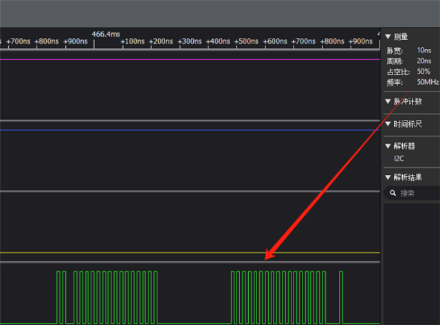
问题1: SN65DSI83 驱动报错如下log,尝试修改过lcd参数,没有任何效果,即便是屏幕不亮,有没有debug验证方法来验证 SN65DSI83转接功能是正常的?比如读写SN65DSI83哪个寄存器?或者测量哪些信号
root@imx8mm-lpddr4-evk:~# dmesg | grep -Ei "Debug|mipi|i2c|drm|sdi|sn65|failed"
[ 0.098335] platform 32e00000.lcdif: Fixed dependency cycle(s) with /soc@0/bus@32c00000/mipi_dsi@32e10000
[ 0.098559] platform 32e00000.lcdif: Fixed dependency cycle(s) with /soc@0/bus@32c00000/mipi_dsi@32e10000
[ 0.098674] platform 32e10000.mipi_dsi: Fixed dependency cycle(s) with /soc@0/bus@30800000/i2c@30a40000/sn65dsi83@2c
[ 0.098702] platform 32e10000.mipi_dsi: Fixed dependency cycle(s) with /soc@0/bus@32c00000/lcdif@32e00000
[ 0.099310] platform 32e40000.usb: Fixed dependency cycle(s) with /soc@0/bus@30800000/i2c@30a30000/tcpc@50/connector
[ 0.103172] platform panel@0: Fixed dependency cycle(s) with /soc@0/bus@30800000/i2c@30a40000/sn65dsi83@2c
[ 0.246847] imx-drm display-subsystem: bound imx-lcdif-crtc.0 (ops lcdif_crtc_ops)
[ 0.279313] i2c_dev: i2c /dev entries driver
[ 0.363694] i2c i2c-0: using DT '/soc@0/bus@30800000/i2c@30a20000' for 'scl' GPIO lookup
[ 0.363717] of_get_named_gpiod_flags: can't parse 'scl-gpios' property of node '/soc@0/bus@30800000/i2c@30a20000[0]'
[ 0.363740] of_get_named_gpiod_flags: can't parse 'scl-gpio' property of node '/soc@0/bus@30800000/i2c@30a20000[0]'
[ 0.363757] i2c i2c-0: using lookup tables for GPIO lookup
[ 0.363764] i2c i2c-0: No GPIO consumer scl found
[ 0.363783] i2c i2c-0: using DT '/soc@0/bus@30800000/i2c@30a20000' for 'sda' GPIO lookup
[ 0.363804] of_get_named_gpiod_flags: can't parse 'sda-gpios' property of node '/soc@0/bus@30800000/i2c@30a20000[0]'
[ 0.363825] of_get_named_gpiod_flags: can't parse 'sda-gpio' property of node '/soc@0/bus@30800000/i2c@30a20000[0]'
[ 0.363841] i2c i2c-0: using lookup tables for GPIO lookup
[ 0.363848] i2c i2c-0: No GPIO consumer sda found
[ 0.364245] i2c i2c-0: IMX I2C adapter registered
[ 0.365239] i2c i2c-1: using DT '/soc@0/bus@30800000/i2c@30a30000' for 'scl' GPIO lookup
[ 0.365274] of_get_named_gpiod_flags: can't parse 'scl-gpios' property of node '/soc@0/bus@30800000/i2c@30a30000[0]'
[ 0.365298] of_get_named_gpiod_flags: can't parse 'scl-gpio' property of node '/soc@0/bus@30800000/i2c@30a30000[0]'
[ 0.365317] i2c i2c-1: using lookup tables for GPIO lookup
[ 0.365324] i2c i2c-1: No GPIO consumer scl found
[ 0.365342] i2c i2c-1: using DT '/soc@0/bus@30800000/i2c@30a30000' for 'sda' GPIO lookup
[ 0.365363] of_get_named_gpiod_flags: can't parse 'sda-gpios' property of node '/soc@0/bus@30800000/i2c@30a30000[0]'
[ 0.365383] of_get_named_gpiod_flags: can't parse 'sda-gpio' property of node '/soc@0/bus@30800000/i2c@30a30000[0]'
[ 0.365397] i2c i2c-1: using lookup tables for GPIO lookup
[ 0.365403] i2c i2c-1: No GPIO consumer sda found
[ 0.368364] i2c i2c-1: IMX I2C adapter registered
[ 0.369351] i2c i2c-2: using DT '/soc@0/bus@30800000/i2c@30a40000' for 'scl' GPIO lookup
[ 0.369385] of_get_named_gpiod_flags: can't parse 'scl-gpios' property of node '/soc@0/bus@30800000/i2c@30a40000[0]'
[ 0.369406] of_get_named_gpiod_flags: can't parse 'scl-gpio' property of node '/soc@0/bus@30800000/i2c@30a40000[0]'
[ 0.369421] i2c i2c-2: using lookup tables for GPIO lookup
[ 0.369428] i2c i2c-2: No GPIO consumer scl found
[ 0.369447] i2c i2c-2: using DT '/soc@0/bus@30800000/i2c@30a40000' for 'sda' GPIO lookup
[ 0.369467] of_get_named_gpiod_flags: can't parse 'sda-gpios' property of node '/soc@0/bus@30800000/i2c@30a40000[0]'
[ 0.369489] of_get_named_gpiod_flags: can't parse 'sda-gpio' property of node '/soc@0/bus@30800000/i2c@30a40000[0]'
[ 0.369507] i2c i2c-2: using lookup tables for GPIO lookup
[ 0.369515] i2c i2c-2: No GPIO consumer sda found
[ 0.369830] platform panel@0: Fixed dependency cycle(s) with /soc@0/bus@30800000/i2c@30a40000/sn65dsi83@2c
[ 0.369954] i2c 2-002c: Fixed dependency cycle(s) with /panel@0
[ 0.370259] sn65dsi83 2-002c: Debug: DT matched - compatible=ti,sn65dsi83, model=0
[ 0.370270] sn65dsi83 2-002c: using DT '/soc@0/bus@30800000/i2c@30a40000/sn65dsi83@2c' for 'enable' GPIO lookup
[ 0.370309] of_get_named_gpiod_flags: parsed 'enable-gpios' property of node '/soc@0/bus@30800000/i2c@30a40000/sn65dsi83@2c[0]' - status (0)
[ 0.370357] sn65dsi83 2-002c: Debug: Enable GPIO acquired successfully
[ 0.377976] nxp-pca9450 0-0025: using DT '/soc@0/bus@30800000/i2c@30a20000/pca9450@25' for 'sd-vsel' GPIO lookup
[ 0.378009] of_get_named_gpiod_flags: can't parse 'sd-vsel-gpios' property of node '/soc@0/bus@30800000/i2c@30a20000/pca9450@25[0]'
[ 0.378036] of_get_named_gpiod_flags: can't parse 'sd-vsel-gpio' property of node '/soc@0/bus@30800000/i2c@30a20000/pca9450@25[0]'
[ 0.381381] sn65dsi83 2-002c: Debug: Parsing device tree for model 0
[ 0.381408] sn65dsi83 2-002c: Debug: Panel bridge (port 2) not ready, deferring probe (ret=-517)
[ 0.381416] sn65dsi83 2-002c: Debug: Failed to parse device tree, ret=-517
[ 0.388532] i2c i2c-2: IMX I2C adapter registered
[ 0.389586] i2c i2c-3: using DT '/soc@0/bus@30800000/i2c@30a50000' for 'scl' GPIO lookup
[ 0.389615] of_get_named_gpiod_flags: can't parse 'scl-gpios' property of node '/soc@0/bus@30800000/i2c@30a50000[0]'
[ 0.389635] of_get_named_gpiod_flags: can't parse 'scl-gpio' property of node '/soc@0/bus@30800000/i2c@30a50000[0]'
[ 0.389651] i2c i2c-3: using lookup tables for GPIO lookup
[ 0.389657] i2c i2c-3: No GPIO consumer scl found
[ 0.389675] i2c i2c-3: using DT '/soc@0/bus@30800000/i2c@30a50000' for 'sda' GPIO lookup
[ 0.389693] of_get_named_gpiod_flags: can't parse 'sda-gpios' property of node '/soc@0/bus@30800000/i2c@30a50000[0]'
[ 0.389711] of_get_named_gpiod_flags: can't parse 'sda-gpio' property of node '/soc@0/bus@30800000/i2c@30a50000[0]'
[ 0.389725] i2c i2c-3: using lookup tables for GPIO lookup
[ 0.389731] i2c i2c-3: No GPIO consumer sda found
[ 0.390166] i2c i2c-3: IMX I2C adapter registered
[ 0.394183] imx-drm display-subsystem: bound imx-lcdif-crtc.0 (ops lcdif_crtc_ops)
[ 0.518539] galcore: clk_get vg clock failed, disable vg!
[ 0.560767] [drm] Initialized vivante 1.0.0 for 38000000.gpu on minor 0
[ 0.571441] sn65dsi83 2-002c: Debug: DT matched - compatible=ti,sn65dsi83, model=0
[ 0.571463] sn65dsi83 2-002c: using DT '/soc@0/bus@30800000/i2c@30a40000/sn65dsi83@2c' for 'enable' GPIO lookup
[ 0.571496] of_get_named_gpiod_flags: parsed 'enable-gpios' property of node '/soc@0/bus@30800000/i2c@30a40000/sn65dsi83@2c[0]' - status (0)
[ 0.571537] sn65dsi83 2-002c: Debug: Enable GPIO acquired successfully
[ 0.582560] sn65dsi83 2-002c: Debug: Parsing device tree for model 0
[ 0.582593] sn65dsi83 2-002c: Debug: Panel bridge (port 2) not ready, deferring probe (ret=-517)
[ 0.582603] sn65dsi83 2-002c: Debug: Failed to parse device tree, ret=-517
[ 0.592182] imx-drm display-subsystem: bound imx-lcdif-crtc.0 (ops lcdif_crtc_ops)
[ 0.593326] sn65dsi83 2-002c: Debug: DT matched - compatible=ti,sn65dsi83, model=0
[ 0.593349] sn65dsi83 2-002c: using DT '/soc@0/bus@30800000/i2c@30a40000/sn65dsi83@2c' for 'enable' GPIO lookup
[ 0.593393] of_get_named_gpiod_flags: parsed 'enable-gpios' property of node '/soc@0/bus@30800000/i2c@30a40000/sn65dsi83@2c[0]' - status (0)
[ 0.593443] sn65dsi83 2-002c: Debug: Enable GPIO acquired successfully
[ 0.604319] sn65dsi83 2-002c: Debug: Parsing device tree for model 0
[ 0.604347] sn65dsi83 2-002c: Debug: Panel bridge (port 2) not ready, deferring probe (ret=-517)
[ 0.604355] sn65dsi83 2-002c: Debug: Failed to parse device tree, ret=-517
[ 0.610644] mmc0: new ultra high speed SDR104 SDIO card at address 0001
[ 0.613636] imx-drm display-subsystem: bound imx-lcdif-crtc.0 (ops lcdif_crtc_ops)
[ 1.647980] systemd[1]: Mounting Kernel Debug File System...
[ 1.719821] systemd[1]: Starting Load Kernel Module drm...
[ 1.885080] systemd[1]: Mounted Kernel Debug File System.
[ 1.933444] systemd[1]: modprobe@drm.service: Deactivated successfully.
[ 1.934051] systemd[1]: Finished Load Kernel Module drm.
[ 10.725256] sn65dsi83 2-002c: Debug: DT matched - compatible=ti,sn65dsi83, model=0
[ 10.725282] sn65dsi83 2-002c: using DT '/soc@0/bus@30800000/i2c@30a40000/sn65dsi83@2c' for 'enable' GPIO lookup
[ 10.725327] of_get_named_gpiod_flags: parsed 'enable-gpios' property of node '/soc@0/bus@30800000/i2c@30a40000/sn65dsi83@2c[0]' - status (0)
[ 10.725380] sn65dsi83 2-002c: Debug: Enable GPIO acquired successfully
[ 10.736713] sn65dsi83 2-002c: Debug: Parsing device tree for model 0
[ 10.736755] sn65dsi83 2-002c: Debug: Panel bridge (port 2) not ready, deferring probe (ret=-517)
[ 10.736764] sn65dsi83 2-002c: Debug: Failed to parse device tree, ret=-517
[ 10.748066] imx-drm display-subsystem: bound imx-lcdif-crtc.0 (ops lcdif_crtc_ops)
[ 10.748967] i2c 2-002c: deferred probe pending: (reason unknown)
root@imx8mm-lpddr4-evk:~# i2cdetect -l
i2c-0 i2c 30a20000.i2c I2C adapter
i2c-1 i2c 30a30000.i2c I2C adapter
i2c-2 i2c 30a40000.i2c I2C adapter
i2c-3 i2c 30a50000.i2c I2C adapter
root@imx8mm-lpddr4-evk:~# i2cdetect -y 2
0 1 2 3 4 5 6 7 8 9 a b c d e f
00: -- -- -- -- -- -- -- --
10: -- -- -- -- -- -- -- -- -- -- -- -- -- -- -- --
20: 20 -- -- -- -- -- -- -- -- -- -- -- 2c -- -- --
30: -- -- -- -- -- -- -- -- -- -- -- -- -- -- -- --
40: -- -- -- -- -- -- -- -- -- -- -- -- -- -- -- --
50: -- -- -- -- -- -- -- -- -- -- -- -- -- -- -- --
60: -- -- -- -- -- -- -- -- -- -- -- -- -- -- -- --
70: -- -- -- -- -- -- -- --
root@imx8mm-lpddr4-evk:~#
问题2 有没有原厂屏幕的购买信息?
想要购买SN65DSI83 转接板的lcd屏幕来验证(排除lcd 屏的差异), 能否提供购买方法?
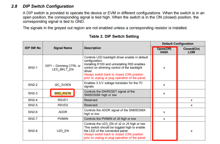
问题3 后续量产硬件连接 ,SN65DSI83 外接的不是屏幕是FPGA 的lvds 接口
SN65DSI83 现有驱动是否支持这种FPGA的连接方式?
3、如下是软硬件环境信息
3.1 硬件环境:
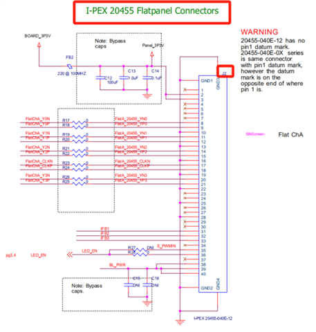
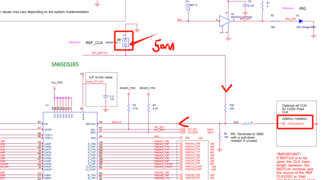
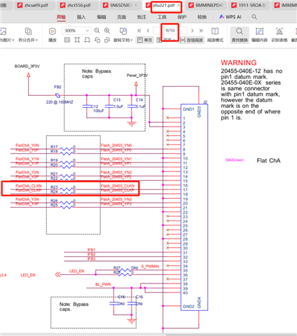
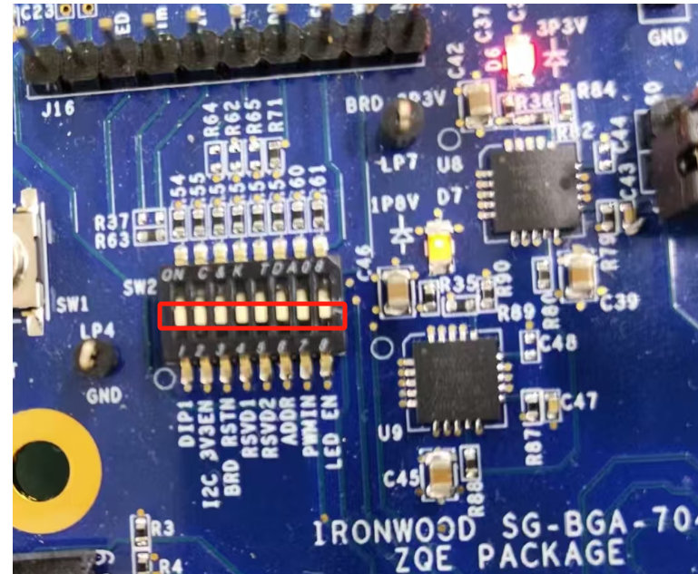
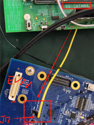
IMX8MM 开发板 MIPI DSI output 接 电平转换后再接TiSN65DSI83官方实验板再飞线接BOE 屏
Imx8侧确认硬件没有问题,换个DSI转HDMI的转接板接显示器可以出图,BOE屏单独测试可以点亮 ,如下连接设置驱动报错
环境连接拓扑如下:
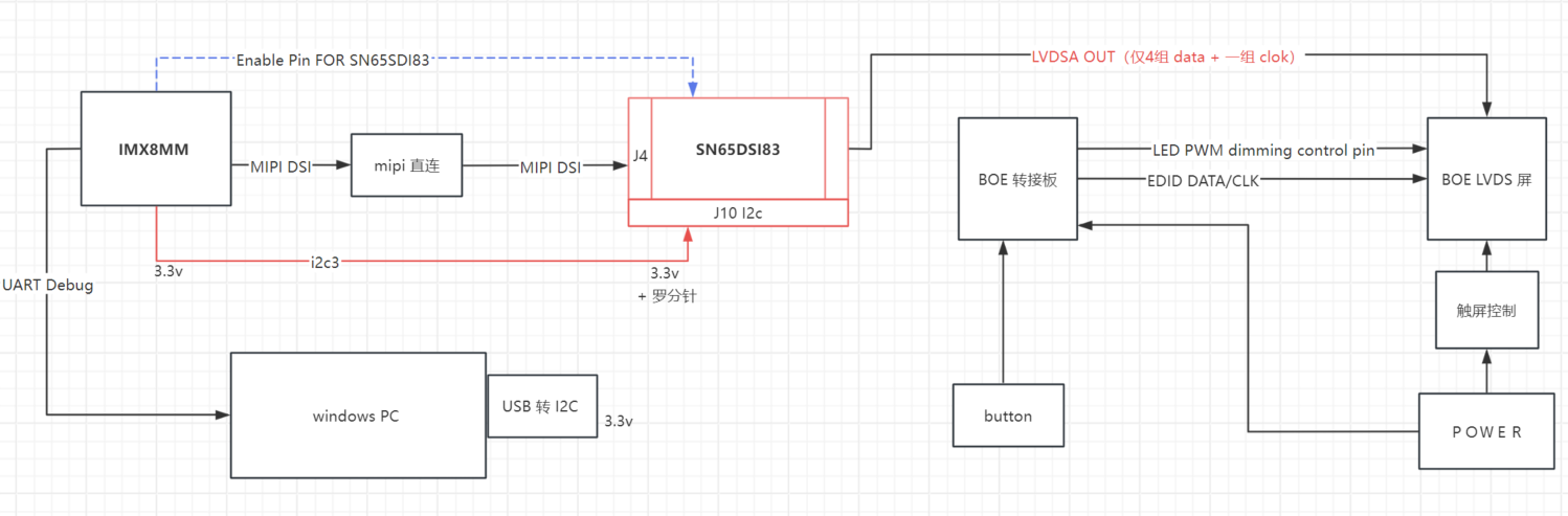
没有找到和SN65DSI83 对应的原厂屏幕,所以采用的飞线的方式接BOE的屏进行测试;
3.2、软件环境:
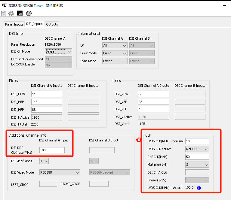
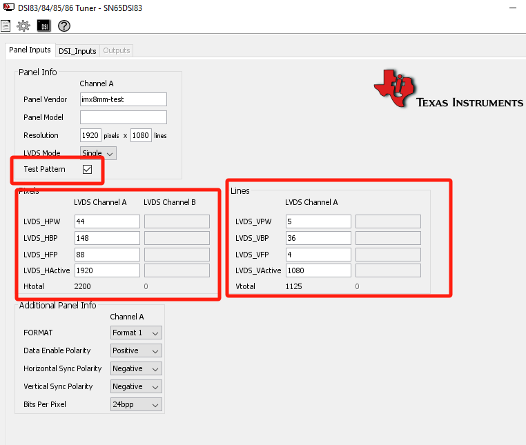
NXP yocto 编译,LINUX 内核版本6.12
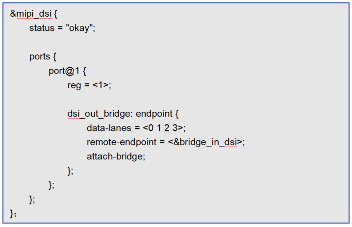
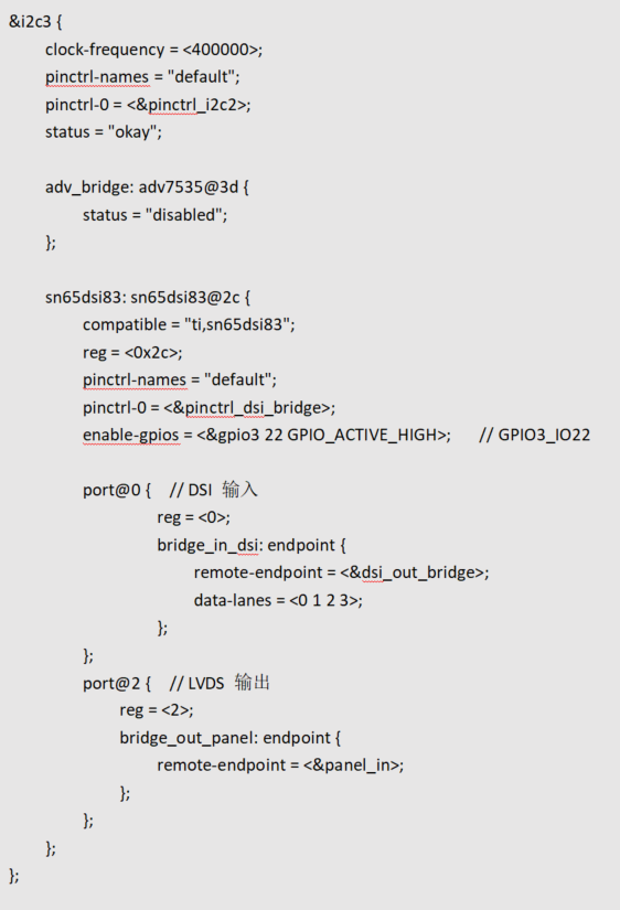
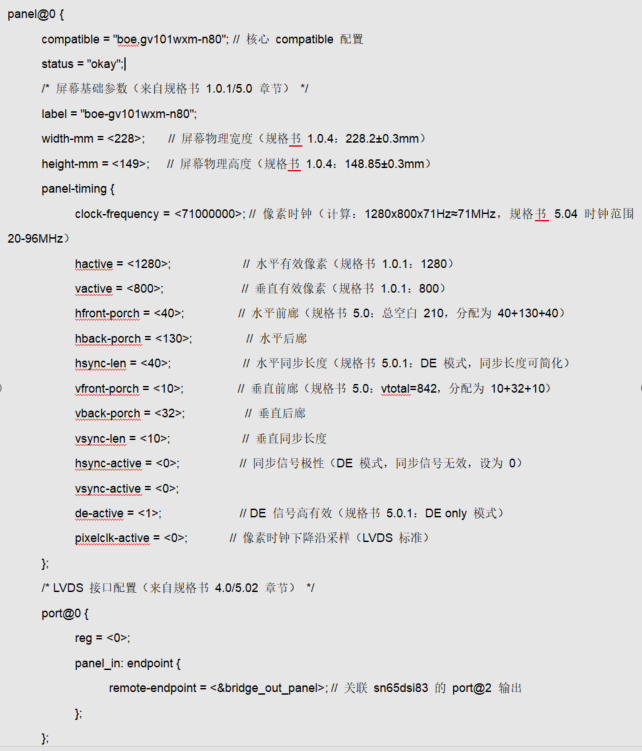
设备树配置如下