This thread has been locked.

If you have a related question, please click the "Ask a related question" button in the top right corner. The newly created question will be automatically linked to this question.

DS90UB941AS-Q1: 进行 Asymmetric Splitting With Cropping 后小的屏幕未能显示

Part Number: DS90UB941AS-Q1

大家好~

需要进行下图所示的分屏和裁剪:
topology

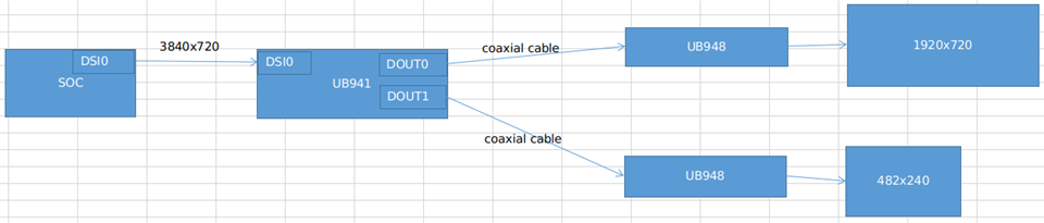
Superframe(执行split之前的帧)的大小为3840x720,
使用UB941的datasheet中的“8.4.6.4.2.1 Asymmetric Splitting With Cropping”章节的方法进行分屏和对Superframe的右侧进行裁剪,
使用RevB_941AS_SuperFrame_Calc.xlsm (snlc064.zip)生成Splitting和Cropping相关的寄存器配置。

遇到的问题是1920x720的屏可以正常显示,但482x240的屏幕不能显示。

试过把Superframe的大小为3840x320并重新配置Splitting和Cropping相关的寄存器,
则482x240的屏幕显示正常,但由于高度大小1920x720的屏幕肯定就显示不正常了。

怀疑过和DOUT1输出的blanking参数有关,在Superframe配置为3840x720时做过尝试:为了使DOUT1输出的blanking能够适配482x240的屏幕,尝试修改过如下的寄存器但没有成功使482x240的屏幕显示出来(我这边对寄存器的理解也是不够,也不确定是否应该更改如下寄存器):
    SPLIT_CLK_SEL, SPLIT_CLK_DIV_M, SPLIT_CLK_DIV_N
    DSI_HSW_CFG_HI, DSI_HSW_CFG_LO, DSI_VSW_CFG_HI, DSI_VSW_CFG_LO
    DSI_PCLK_DIV_M, DSI_PCLK_DIV_N

查看的datasheet为“DS90UB941AS-Q1 DSI to FPD-Link III Bridge Serializer datasheet (Rev. C)”。

调试时使用的Superframe的timing配置为:
    uVisWidth        = '3840'
    uHsyncFrontPorch = '128'
    uHsyncWidth      = '128'
    uHsyncBackPorch  = '128'
    uVisHeight       = '720'
    uVsyncFrontPorch = '3'
    uVsyncWidth      = '3'
    uVsyncBackPorch  = '3'
    uPixelFreqInHz   = '184757760'
    bDEPolarity      = '0'

482x240的屏幕timing specification如下图:
timing_of_small_display
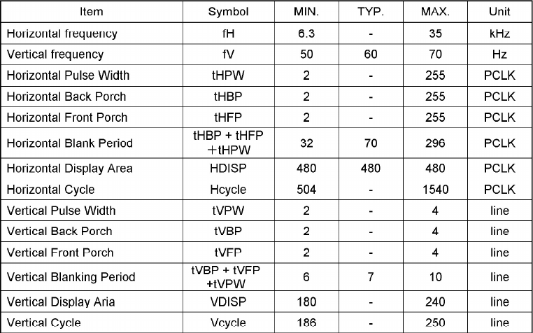
(虽然上图中的hWidth是480,但由于bug,把hWidth设置为480会在一侧显示异常的白色竖线,所以现在设置的是482)

目前的UB941的寄存器配置如下:

    0x01=0x08    #  Disable DSI */
    0x1e=0x01    #  Select FPD-Link III Port 0*/
    0x06=0x01    #  Change deser i2c addr */
    0x07=0x58
    0x08=0x5A
    0x03=0x9a    #  Enable I2C_PASSTHROUGH */
    0xc6=0x21    #  Step 1 of "8.3.8.1 Interrupt Pin (INTB)" from datasheet */
    0x40=0x04    #  Select DSI Port 0 digital registers */
    0x41=0x21    #  Select DSI_CONFIG_1 register */
    0x42=0x60    #  Set DSI_VS_POLARITY=DSI_HS_POLARITY=1 */

    0x1E=0x01    #  Select Port0  # set split mode, left/right 3D image, non-continuous clock mode
    0x5B=0x87    #  Force Splitter Mode
    0x56=0x80    #  Enable conversion of L/R image into alternating pixel image
    0x4F=0x84    #  Set 2 lane DSI
    0x1E=0x02    #  Select Port1
    0x5B=0x87    #  Force Splitter Mode
    0x56=0x80    #  Enable conversion of L/R image into alternating pixel image
    0x4F=0x84    #  Set 2 lane DSI

    0x06=0x01    #  Change deser i2c addr */
    0x07=0x58
    0x08=0x5E
    0x03=0x9a    #  Enable I2C_PASSTHROUGH */
    0xc6=0x21    #  Step 1 of "8.3.8.1 Interrupt Pin (INTB)" from datasheet */
    0x40=0x08    #  Select DSI Port 1 digital registers */
    0x41=0x21    #  Select DSI_CONFIG_1 register */
    0x42=0x60    #  Set DSI_VS_POLARITY=DSI_HS_POLARITY=1 */

    0x1E=0x01    #  Select Port0

    0x32=0x80    #  Set IMG_LINE_SIZE
    0x33=0x07    #  Set IMG_LINE_SIZE
    0x36=0x00    #  Set crop start X position (LSB)
    0x37=0x80    #  Set crop start X position (MSB)
    0x38=0x7F    #  Set crop stop X position (LSB)
    0x39=0x07    #  Set crop stop X position (MSB)
    0x3A=0x00    #  Set crop start Y position (LSB)
    0x3B=0x00    #  Set crop start Y position (MSB)
    0x3C=0xCF    #  Set crop stop Y position (MSB)
    0x3D=0x02    #  Set crop start Y position (LSB)

    0x1E=0x02    #  Select Port1

    0x36=0x00    #  Set crop start X position (LSB)
    0x37=0x80    #  Set crop start X position (MSB)
    0x38=0xE1    #  Set crop stop X position (LSB)
    0x39=0x01    #  Set crop stop X position (MSB)
    0x3A=0x00    #  Set crop start Y position (LSB)
    0x3B=0x00    #  Set crop start Y position (MSB)
    0x3C=0xEF    #  Set crop stop Y position (MSB)
    0x3D=0x00    #  Set crop start Y position (LSB)

    0x1E=0x01    #  Select Port0
    0x40=0x04    #  Select DSI digital page
    0x41=0x05    #  To reg 0x05 (TSKIP CNT)
    0x42=0x36    #  Set value for DSI+CLK
    0x40=0x08    #  Select DSI digital page
    0x41=0x05    #  To reg 0x05 (TSKIP CNT)
    0x42=0x36    #  Set value for DSI+CLK

    0x01=0x00    #  Enable DSI */

现有如下问题:
1. 按第1个图那样进行分屏和裁剪后,UB941的datasheet中说的意思我理解是vertical blanking会变的很大,但具体变为什么样子我不太清楚,所以请问DOUT1输出的display timing / blanking的值是怎样的?
2. UB941支持对DOUT1输出的display timing / blanking进行修改吗?支持的话如何配置?
3. 还需要做什么才能使两个屏幕都能正常显示?

  • 您好,关于您的这个问题,我需要再确认以下,给您带来不便非常抱歉.

  • Kailyn Chen 您好,

    我找到了您在英文论坛发的帖子:
        e2e.ti.com/.../ds90ub941as-q1-dsi-data-lane-with-480-240-display-monitor-questions
    以及之前我发过的帖子的对应的英文帖子:
        e2e.ti.com/.../ds90ub941as-q1-asymmetric-splitting-with-cropping-questions

    我现在有如下疑问:

    1.
    Since the vertical blanking can't be removed, the current application should not be feasible, but what if splitter mode changes to "Asymmetric Splitting With DSI VC-IDs", is it possible to drive the two screens with one DSI input?
    (I see the following description from section of "Asymmetric Splitting With DSI VC-IDs":
        Vertical blanking for resultant video streams with virtual channels is the same as with superframe implementation, hence the smaller video stream will have larger vertical blanking.
    But I managed to drive the smaller screen with 11.64.MHz PCLK (e2e.ti.com/.../ds90ub941as-q1-asymmetric-splitting-with-cropping-questions), so I think not all descriptions in the datasheet are accurate and I'd like to do some tryings.)

    2.
    I heard that there is UB981, is UB981 able to adjust vertical blanking?

  • 我的帐号无法在英文论坛发帖,会提示:
    To post on TI E2ETm design support forums, you must have a valid company email address in your myTI account. If you have a valid company email address, please add it to your account by following the instructions in the myTI account FAQ (Note: there may be an ~10 minute delay for this email change to propagate to all necessary systems). If you don’t, we encourage you to search the TI E2E design support forums for existing answers.

  • 您好,是的,美国工程师的意思是,按照提供的这个panel的规格,是无法实现这种分割的。他给出的方案是使用独立的2:2输入模式,提供两个独立的DSI输入给941AS ,然后独立输出两个不同分辨率的视频。

  • Kailyn Chen 您好,

    谢谢回复~
    然后麻烦看看我发的第2个comment中的两个问题能否回复一下,谢谢。

  • 您好,981因为属于NDA的产品,所以暂时没有资料可以参考,我这边针对您的两个问题,再确认下。 给您带来不便非常抱歉。

  • Hello, about the question about the vertical blanking, please refer to the reply of our foreign engineer:

    As the datasheet mentions, the vertical blanking implications for VCID-based splitting are the same as for superframe splitting so you would have the same issue there. Also please note that 941AS has a minimum PCLK rate of 25MHz, so you may have gotten 11.64MHz to work as stated above, but this is not expected to operate over device PVT conditions so we would not advise using that configuration. 

    The superframe splitting on this part is generally most useful for driving asymmetric screens which have similar vertical dimensions or for driving panels which have a wide range of tolerance in the vertical blanking/PCLK. 

    For example an easy split to implement would be 1920x720 plus 1280x720 since they have the same vertical dimension.