

Hi Ti Team:
I have a question about the SN6505B chip as follows:
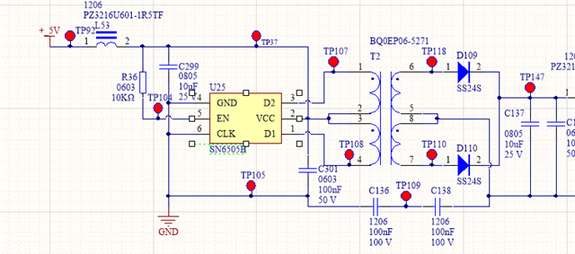
Schematic diagram:
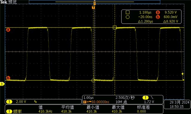
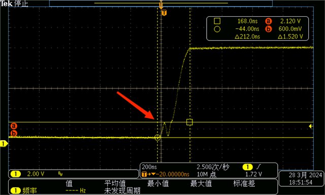
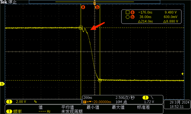
I found that the rising and falling waveforms of the D1 and D2 pins of the actual test chip have a kickback. Is this normal?
Hi Ti Team:
I have a question about the SN6505B chip as follows:
Schematic diagram:
I found that the rising and falling waveforms of the D1 and D2 pins of the actual test chip have a kickback. Is this normal?
【求助】使用SN6505搭建5V转20V隔离电源(数据手册第27页参考电路),SN6505本身的功率损耗和效率应该如何计算呢?
需要利用功率损耗参数来计算结温温升。求大神解惑!!!
您好,我想问下SN6505B推挽变换器为什么和传统的推挽拓扑不同,其输出侧怎么没有滤波电感只有滤波电容?如果没有滤波电感那么变换器的输入输出电压满足什么公式?