

主题中讨论的其他部件:C2000WARE
大家好,
使用CCS 10.4 ,我将I2C功能添加到一个项目中,这个项目以TIREX示例“Example_2802xScia_FFDLB.c”开始,如下所示:
//#############################################################################
//
//  File:   Example_F2802xSci_FFDLB.c
//
//  Title:  F2802x Device SCI FIFO Digital Loop Back Test.
//
//! \addtogroup example_list
//!  <h1>SCI FIFO Digital Loop Back</h1>
//!
//!   This test uses the loopback test mode of the SCI module to send
//!   characters starting with 0x00 through 0xFF.  The test will send
//!   a character and then check the receive buffer for a correct match.
//!
//!   Watch Variables:
//!   - LoopCount - Number of characters sent
//!   - ErrorCount - Number of errors detected
//!   - SendChar - Character sent
//!   - ReceivedChar - Character received
//
//#############################################################################
// $TI Release:  $
// $Release Date:  $
// $Copyright:
// Copyright (C) 2009-2022 Texas Instruments Incorporated - http://www.ti.com/
//
// Redistribution and use in source and binary forms, with or without
// modification, are permitted provided that the following conditions
// are met:
//
//   Redistributions of source code must retain the above copyright
//   notice, this list of conditions and the following disclaimer.
//
//   Redistributions in binary form must reproduce the above copyright
//   notice, this list of conditions and the following disclaimer in the
//   documentation and/or other materials provided with the
//   distribution.
//
//   Neither the name of Texas Instruments Incorporated nor the names of
//   its contributors may be used to endorse or promote products derived
//   from this software without specific prior written permission.
//
// THIS SOFTWARE IS PROVIDED BY THE COPYRIGHT HOLDERS AND CONTRIBUTORS
// "AS IS" AND ANY EXPRESS OR IMPLIED WARRANTIES, INCLUDING, BUT NOT
// LIMITED TO, THE IMPLIED WARRANTIES OF MERCHANTABILITY AND FITNESS FOR
// A PARTICULAR PURPOSE ARE DISCLAIMED. IN NO EVENT SHALL THE COPYRIGHT
// OWNER OR CONTRIBUTORS BE LIABLE FOR ANY DIRECT, INDIRECT, INCIDENTAL,
// SPECIAL, EXEMPLARY, OR CONSEQUENTIAL DAMAGES (INCLUDING, BUT NOT
// LIMITED TO, PROCUREMENT OF SUBSTITUTE GOODS OR SERVICES; LOSS OF USE,
// DATA, OR PROFITS; OR BUSINESS INTERRUPTION) HOWEVER CAUSED AND ON ANY
// THEORY OF LIABILITY, WHETHER IN CONTRACT, STRICT LIABILITY, OR TORT
// (INCLUDING NEGLIGENCE OR OTHERWISE) ARISING IN ANY WAY OUT OF THE USE
// OF THIS SOFTWARE, EVEN IF ADVISED OF THE POSSIBILITY OF SUCH DAMAGE.
// $
//#############################################################################

//
// Included Files
//
#include "DSP28x_Project.h"     // Device Headerfile and Examples Include File
#include <stdio.h>
#include <file.h>

#include "common/include/adc.h"
#include "common/include/clk.h"
#include "common/include/flash.h"
#include "common/include/gpio.h"
#include "common/include/pie.h"
#include "common/include/pll.h"
#include "common/include/sci.h"
#include "common/include/wdog.h"

//
// Function Prototypes
//
void scia_init(void);
void scia_fifo_init(void);
void scia_xmit(int a);
void error(void);

//
// Globals
//
uint16_t LoopCount;
uint16_t ErrorCount;

ADC_Handle myAdc;
CLK_Handle myClk;
FLASH_Handle myFlash;
GPIO_Handle myGpio;
PIE_Handle myPie;
SCI_Handle mySci;

//
// Main
//
void main(void)
{
    uint16_t SendChar;
    uint16_t ReceivedChar;

    CPU_Handle myCpu;
    PLL_Handle myPll;
    WDOG_Handle myWDog;

    //
    // Initialize all the handles needed for this application
    //
    myAdc = ADC_init((void *)ADC_BASE_ADDR, sizeof(ADC_Obj));
    myClk = CLK_init((void *)CLK_BASE_ADDR, sizeof(CLK_Obj));
    myCpu = CPU_init((void *)NULL, sizeof(CPU_Obj));
    myFlash = FLASH_init((void *)FLASH_BASE_ADDR, sizeof(FLASH_Obj));
    myGpio = GPIO_init((void *)GPIO_BASE_ADDR, sizeof(GPIO_Obj));
    myPie = PIE_init((void *)PIE_BASE_ADDR, sizeof(PIE_Obj));
    myPll = PLL_init((void *)PLL_BASE_ADDR, sizeof(PLL_Obj));
    mySci = SCI_init((void *)SCIA_BASE_ADDR, sizeof(SCI_Obj));
    myWDog = WDOG_init((void *)WDOG_BASE_ADDR, sizeof(WDOG_Obj));

    //
    // Perform basic system initialization
    //
    WDOG_disable(myWDog);
    CLK_enableAdcClock(myClk);
    (*Device_cal)();

    //
    // Select the internal oscillator 1 as the clock source
    //
    CLK_setOscSrc(myClk, CLK_OscSrc_Internal);

    //
    // Setup the PLL for x10 /2 which will yield 50Mhz = 10Mhz * 10 / 2
    //
    PLL_setup(myPll, PLL_Multiplier_10, PLL_DivideSelect_ClkIn_by_2);

    //
    // Disable the PIE and all interrupts
    //
    PIE_disable(myPie);
    PIE_disableAllInts(myPie);
    CPU_disableGlobalInts(myCpu);
    CPU_clearIntFlags(myCpu);

    //
    // If running from flash copy RAM only functions to RAM
    //
#ifdef _FLASH
    memcpy(&RamfuncsRunStart, &RamfuncsLoadStart, (size_t)&RamfuncsLoadSize);
#endif

    //
    // Setup GPIO
    //
    GPIO_setPullUp(myGpio, GPIO_Number_28, GPIO_PullUp_Enable);
    GPIO_setPullUp(myGpio, GPIO_Number_29, GPIO_PullUp_Disable);
    GPIO_setQualification(myGpio, GPIO_Number_28, GPIO_Qual_ASync);
    GPIO_setMode(myGpio, GPIO_Number_28, GPIO_28_Mode_SCIRXDA);
    GPIO_setMode(myGpio, GPIO_Number_29, GPIO_29_Mode_SCITXDA);

    //
    // Setup a debug vector table and enable the PIE
    //
    PIE_setDebugIntVectorTable(myPie);
    PIE_enable(myPie);

    LoopCount = 0;
    ErrorCount = 0;

    scia_init();                // Initialize SCI for digital loop back
    scia_fifo_init();           // Initialize the SCI FIFO

    //
    // Send a character starting with 0
    //
    SendChar = 0;

    //
    // Send Characters forever starting with 0x00 and going through 0xFF.
    // After sending each, check the receive buffer for the correct value
    //
    for(;;)
    {
        SCI_putDataBlocking(mySci, SendChar);

        while(SCI_getRxFifoStatus(mySci) == SCI_FifoStatus_Empty)
        {

        }

        //
        // Check received character
        //
        ReceivedChar = SCI_getData(mySci);
        if(ReceivedChar != SendChar)
        {
            error();
        }

        //
        // Move to the next character and repeat the test
        //
        SendChar++;

        //
        // Limit the character to 8-bits
        //
        SendChar &= 0x00FF;
        LoopCount++;
    }
}

//
// Step 7. Insert all local Interrupt Service Routines (ISRs) and
// functions here:
//

//
// error -
//
void
error(void)
{
    ErrorCount++;
    __asm(" ESTOP0");       // Uncomment to stop the test here
    for (;;)
    {

    }

}

//
// scia_init -
//
void
scia_init()
{
    CLK_enableSciaClock(myClk);

    //
    // 1 stop bit,  No loopback, No parity,8 char bits, async mode,
    // idle-line protocol
    //
    SCI_disableParity(mySci);
    SCI_setNumStopBits(mySci, SCI_NumStopBits_One);
    SCI_setCharLength(mySci, SCI_CharLength_8_Bits);

    //
    // enable TX, RX, internal SCICLK, Disable RX ERR, SLEEP, TXWAKE
    //
    SCI_enableTx(mySci);
    SCI_enableRx(mySci);
    SCI_enableTxInt(mySci);
    SCI_enableRxInt(mySci);

    SCI_enableLoopBack(mySci);

    //SCI BRR = LSPCLK/(SCI BAUDx8) - 1
#if (CPU_FRQ_50MHZ)
    SCI_setBaudRate(mySci, SCI_BaudRate_9_6_kBaud);
#elif (CPU_FRQ_40MHZ)
    SCI_setBaudRate(mySci, (SCI_BaudRate_e)129);
#endif

    SCI_enable(mySci);

    return;
}

//
// scia_fifo_init - Initialize the SCI FIFO
//
void
scia_fifo_init()
{
    SCI_enableFifoEnh(mySci);
    SCI_resetTxFifo(mySci);
    SCI_clearTxFifoInt(mySci);
    SCI_resetChannels(mySci);
    SCI_setTxFifoIntLevel(mySci, SCI_FifoLevel_Empty);

    SCI_resetRxFifo(mySci);
    SCI_clearRxFifoInt(mySci);
    SCI_setRxFifoIntLevel(mySci, SCI_FifoLevel_4_Words);

    return;
}

//
// End of File
//
此代码及其包含的项目是从以下路径中的资源资源管理器导入的:
/Software/C2000Ware (4.01 .00.00)/English/Devices/F2802x/F28020/Examples/DriverLib/scia_loopback/Example_2802xScia_FFDLB.c</s>2.802万 2802
SCIA通信运行良好,现在我尝试添加简单的I2C写入功能。
另外,我还修改了C2000Ware的Bitfiled Example_2802xI2C_EEPROM.c,以满足I2C需求,而且工作正常。 现在我将功能从I2C位域示例移到SCIA Driverlib示例代码中。
完成后,RS232命令将通过SCIA模块接收,解析,并通过I2C发送到外围设备。
第一步是将I2C初始化函数插入到SCIA Driverlib示例代码中。 下面是我创建并插入的功能:
//
// Start I2C_init() Initialization Routine
//
void
I2C_init()
{
    EALLOW;

    // Initialize I2C
    I2caRegs.I2CMDR.bit.IRS         = 0;    // SEE BELOW - Put I2C module in reset while making changes

    //
    // Own Address Register
    //                              // Bit   15: READ ONLY - Reserved
    I2caRegs.I2COAR                 = 0x40; // Own address = 0x40
    I2caRegs.I2CSAR                 = 0x44; // Bits   0-9: Address to which data will be transmitted (Master only)

/*                                                                        // Bits 7-15: Reserved
    //
    // I2C Interrupt Enable Register
    //
#ifdef BIT_SET_REGISTERS
    // Bits 7-15: READ ONLY - Reserved
    I2caRegs.I2CIER.bit.AAS         = 0;    // Bit   6: 1 = Addressed as slave interrupt request enabled
    I2caRegs.I2CIER.bit.SCD         = 0;    // Bit     5: 1 = Stop condition detected interrupt request enabled
    I2caRegs.I2CIER.bit.XRDY        = 0;    // Bit     4: 1 = Transmit data ready interrupt request disabled
    I2caRegs.I2CIER.bit.RRDY        = 0;    // Bit     3: 1 = W1C - Receive data ready interrupt request enabled
    I2caRegs.I2CIER.bit.ARDY        = 0;    // Bit     2: 1 = Master Only - Register access ready interrupt request enabled
    I2caRegs.I2CIER.bit.NACK        = 0;    // Bit     1: 0 = W1C - No-ack interrupt request disabled
    I2caRegs.I2CIER.bit.ARBL        = 0;    // Bit     0: 0 = W1C - Arbitration lost interrupt request disabled
#else
    I2caRegs.I2CIER.all             = 0x0000;    // Per above bit settings
#endif


    //
    // I2C Status Register
    //
#ifdef BIT_SET_REGISTERS
    // Bit   15: READ ONLY - Reserved
    I2caRegs.I2CSTR.bit.SDIR        = 0;    // Bit   14: W1C - Slave direction bit 0 = not addressed as slave transmitter
    I2caRegs.I2CSTR.bit.NACKSNT     = 0;    // Bit   13: W1C - NACK sent bit 0 = NACK not sent
    I2caRegs.I2CSTR.bit.BB          = 0;    // Bit   12: Bus Busy bit 0 = bus free
    I2caRegs.I2CSTR.bit.RSFULL      = 0;    // Bit   11: 1 = receive shift register overrun condition detected
    I2caRegs.I2CSTR.bit.XSMT        = 0;    // Bit   10: 0 = transmit shift register underflow detected (empty)
    I2caRegs.I2CSTR.bit.AAS         = 0;    // Bit    9: 1 = I2C module recognized its own slave address
    I2caRegs.I2CSTR.bit.AD0         = 0;    // Bit    8: 1 = address of all zeros (general call) was detected
    // Bits 6-7: READ ONLY - Reserved
    I2caRegs.I2CSTR.bit.SCD         = 0;    // Bit    5: W1C - 1 = stop condition was detected
    I2caRegs.I2CSTR.bit.XRDY        = 0;    // Bit    4: 1 = Ready for more transmit data to go in I2CDXR
    I2caRegs.I2CSTR.bit.RRDY        = 0;    // Bit    3: W1C - Receive data ready int flag 1 = data is in I2CDRR
    I2caRegs.I2CSTR.bit.ARDY        = 0;    // Bit    2: Master Only - Register access ready int flag
    I2caRegs.I2CSTR.bit.NACK        = 0;    // Bit    1: W1C - 1 = NACK received
    I2caRegs.I2CSTR.bit.ARBL        = 0;    // Bit    0: W1C - 1 = arbitration lost
#else
    I2caRegs.I2CSTR.all             = 0x0000;    // Per above bit settings
#endif


    //
    // I2C Clock Prescale Register
    //
    // Setup I2C data rate
    I2caRegs.I2CPSC.bit.IPSC        = 5;    // Prescaler value 60mHz SYSCLK / 6 = 10mHz (5+1=6)


    //
    // I2C Clock high-time and low-time Registers
    //
    // 10mHz / 200 = 50kHz for comm's with 2x16 debugging display
    I2caRegs.I2CCLKL                =  129; // 129 + 5 = 136
    I2caRegs.I2CCLKH                =   61; //  61 + 5 =  66


    //
    // Data Count Register
    //
    I2caRegs.I2CCNT                 = 0;    // Bits 0-15: Set data count (ignored in RM mode)
                                    // Is changed to actual number of bytes to transfer when in
                                    // transmit mode.
    //
    // Slave Address Register
    //                                                           // Bits 10-15: READ ONLY - Reserved
    I2caRegs.I2CSAR                 = 0x44; // Bits   0-9: Address to which data will be transmitted (Master only)

    //
    // Data transmit register
    //
    I2caRegs.I2CDXR = 0x00;

    //
    // I2C Mode Register
    //
#ifdef BIT_SET_REGISTERS
    // Bits 14-15:  READ ONLY - Reserved
    I2caRegs.I2CMDR.bit.NACKMOD     = 0;    // Bit   15: NACK mode
    I2caRegs.I2CMDR.bit.FREE        = 0;    // Bit   14: For debugging: 0 = I2C halts during interrupts
//  I2caRegs.I2CMDR.bit.STT         = 0;    // Bit   13: Master only - Start bit Can't be written when IRS=0
    // Bit   12: Reserved
//  I2caRegs.I2CMDR.bit.STP         = 0;    // Bit   11: Master only - Stop bit Can't be written when IRS=0
    I2caRegs.I2CMDR.bit.MST         = 1;    // Bit   10: Remains 0 for slave mode.  1 = Master mode
    I2caRegs.I2CMDR.bit.TRX         = 1;    // Bit    9: 0 = Receive mode, 1 = Transmit mode
    I2caRegs.I2CMDR.bit.XA          = 0;    // Bit    8: 0 = 7 bit address mode
    I2caRegs.I2CMDR.bit.RM          = 1;    // Bit    7: 1 = repeat mode
    I2caRegs.I2CMDR.bit.DLB         = 0;    // Bit    6: 0 = Digital loopback mode disabled
//  I2caRegs.I2CMDR.bit.IRS         = 1;    // Bit    5: I2C module is re-enabled after making changes
    I2caRegs.I2CMDR.bit.STB         = 0;    // Bit    4: Master only - Start Byte mode
    I2caRegs.I2CMDR.bit.FDF         = 0;    // Bit    3: Keep at 0. Free data format mode
    I2caRegs.I2CMDR.bit.BC          = 0;    // Bits 0-2: Set bit count to 8 bits (0 = 8)
#else
    I2caRegs.I2CMDR.all             = 0x06a0;    // Per above bit settings
#endif


    //
    // I2C Extended Mode Register
    //                                                           // Bits 1-15: READ ONLY - Reserved
    I2caRegs.I2CEMDR.bit.BCM         = 0;   // Bit     0: Backwards compatibility mode


    //
    // Transmit FIFO Register
    //
#ifdef BIT_SET_REGISTERS
    // Bits 14-15:  READ ONLY - Reserved
    // Bit 15: Reserved
    I2caRegs.I2CFFTX.bit.I2CFFEN    = 0;    // Bit    14: 1 = Enable transmit & receive FIFOs
    I2caRegs.I2CFFTX.bit.TXFFRST    = 0;    // Bit    13: 1 = Take transmit FIFO out of reset
//  I2caRegs.I2CFFTX.bit.TXFFST     = 0;    // Bits 8-12: READ ONLY - How many bytes are in the transmit FIFO
//  I2caRegs.I2CFFTX.bit.TXFFINT    = 0;    // Bit     7: READ ONLY - 1 = interrupt occurred
    I2caRegs.I2CFFTX.bit.TXFFINTCLR = 0;    // Bit     6: W1C - Clears transmit interrupt flag (do again after irs = 1)
    I2caRegs.I2CFFTX.bit.TXFFIENA   = 0;    // Bit     5: 0 = Disable transmit FIFO interrupt
    I2caRegs.I2CFFTX.bit.TXFFIL     = 0;    // Bits  0-4: Set the transmit FIFO interrupt Threshold
#else
    I2caRegs.I2CFFTX.all            = 0x0000;    // Per above bit settings
#endif


    //
    // Receive FIFO Register
    //
#ifdef BIT_SET_REGISTERS
    // Bits 14-15:  READ ONLY - Reserved
    I2caRegs.I2CFFRX.bit.RXFFRST    = 0;    // Bit     13: 1 = enable receive FIFO operation
//  I2caRegs.I2CFFRX.bit.RXFFST     = 0;    // BitS  8-12: READ ONLY - Bytes in receive FIFO
//  I2caRegs.I2CFFRX.bit.RXFFINT    = 0;    // Bit      7: READ ONLY - Receive interrupt flag 1 = int
    I2caRegs.I2CFFRX.bit.RXFFINTCLR = 0;    // Bit      6: Write 1 to clear receive int flag
    I2caRegs.I2CFFRX.bit.RXFFIENA   = 0;    // Bit      5: 1 = receive interrupt is enabled
    I2caRegs.I2CFFRX.bit.RXFFIL     = 0;    // Bits   0-4: Set the receive FIFO interrupt level
#else
    I2caRegs.I2CFFRX.all            = 0x0000;    // Per above bit settings
#endif
*/

    // Clean up and exit
    I2caRegs.I2CMDR.bit.IRS         = 1;    // SEE ABOVE - I2C module is re-enabled after making changes

    EDIS;
    return;
}
/*
 * End I2C_init()
 */
从上面的代码中可以看出,我尝试将每个寄存器设置为一个位,并尝试设置每个寄存器一个字。
该代码编译没有问题,上载到目标并正常运行,除了I2C寄存器没有更改。
代码运行,因此我在寄存器更改时设置了一个断点,然后逐步执行几行,这些行应该更改寄存器值。 观察“寄存器”视图和“内存浏览器”视图时,没有发生任何变化。
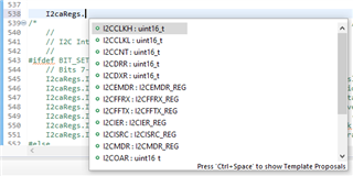
当我输入要写入寄存器的代码时,CCS将标识该寄存器的各种元素,我可以从列表中选择这些元素以自动填充:
问题:
1.此问题是否是由于将Bitfiled示例代码与Driverlib代码组合而导致的?
2.我是否遗漏了一些包含的内容?
3.在寄存器中写入数据以设置其值的正确方式是什么?
谢谢!
罗宾
