This thread has been locked.

If you have a related question, please click the "Ask a related question" button in the top right corner. The newly created question will be automatically linked to this question.

[参考译文] LAUNCHXL-F280049C:将16位 SPI 通信代码转换为24位

Guru**** 2382630 points
Other Parts Discussed in Thread: DRV8316, C2000WARE, DRV8311, DRV8376
请注意,本文内容源自机器翻译,可能存在语法或其它翻译错误,仅供参考。如需获取准确内容,请参阅链接中的英语原文或自行翻译。

https://e2e.ti.com/support/microcontrollers/c2000-microcontrollers-group/c2000/f/c2000-microcontrollers-forum/1421059/launchxl-f280049c-converting-16-bit-spi-communication-code-to-24-bits

器件型号:LAUNCHXL-F280049C
主题中讨论的其他器件:C2000WAREDRV8311DRV8376、DRV8316

工具与软件:

您好!

我已经在这方面工作了一段时间,我真的很困倦,所以任何帮助都会被感激!

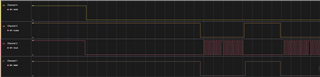
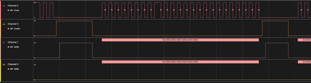
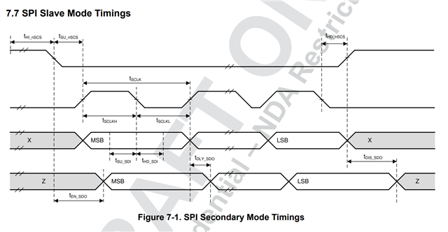
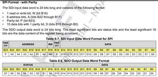
我有一个代码可以与具有16位 SPI 帧的 DRV 器件通信、我正在尝试更改此代码、以便可以与具有24位 SPI 帧的另一个 DRV 器件通信。

以下是我之前尝试转换的 SPI 帧的当前代码:

void Config_evm_spi(void)
{
    //Pin Config
    EALLOW;
    // SPI_MOSI
    GPIO_SetupPinOptions(16, GPIO_INPUT, GPIO_ASYNC | GPIO_PULLUP);
    // SPI_MISO
    GPIO_SetupPinOptions(17, GPIO_INPUT, GPIO_ASYNC | GPIO_PULLUP);
    // SPI_CS
    GPIO_SetupPinOptions(56, GPIO_INPUT, GPIO_ASYNC | GPIO_PULLUP);
    // SPI_CLK
    GPIO_SetupPinOptions(57, GPIO_INPUT, GPIO_ASYNC | GPIO_PULLUP);

    GPIO_SetupPinMux(16, GPIO_MUX_CPU1, 1);
    GPIO_SetupPinMux(17, GPIO_MUX_CPU1, 1);
    GPIO_SetupPinMux(56, GPIO_MUX_CPU1, 1);
    GPIO_SetupPinMux(57, GPIO_MUX_CPU1, 1);
    EDIS;

    EALLOW;
    ClkCfgRegs.LOSPCP.all = 0;
    EDIS;

    // Initialize SPI FIFO registers
    SpiaRegs.SPIFFTX.all=0xE040;
    SpiaRegs.SPIFFRX.all=0x2044;
    SpiaRegs.SPIFFCT.all=0x0;

    //SPI Settings
    SpiaRegs.SPICCR.bit.SPISWRESET = 0;     //SPI Reset On
    SpiaRegs.SPICCR.bit.CLKPOLARITY = 0;    //SCLK Active High
    SpiaRegs.SPICCR.bit.SPICHAR = 0xF;      //16-bit SPI char
    SpiaRegs.SPICCR.bit.SPILBK = 0;

    SpiaRegs.SPICTL.bit.OVERRUNINTENA = 0;  //No overrun interrupt
    SpiaRegs.SPICTL.bit.CLK_PHASE = 0;      //Phase 0
    SpiaRegs.SPICTL.bit.MASTER_SLAVE = 1;   //Master mode
    SpiaRegs.SPICTL.bit.TALK = 1;           //nSCS enabled
    SpiaRegs.SPICTL.bit.SPIINTENA = 0;      //TX/RX Interrupt Disabled

    SpiaRegs.SPIBRR.bit.SPI_BIT_RATE = ((25000000 / 1000000) - 1);              //Set baud rate to 1MHz
    SpiaRegs.SPIPRI.bit.FREE = 1;           //Set so breakpoints don't disturb transmission
    SpiaRegs.SPICCR.bit.SPISWRESET = 1;   //Exit SPI reset

}

Uint16 spi_xmit(Uint16 spiFrame)
{
    SpiaRegs.SPITXBUF=spiFrame;

    //Wait for RX flag to indicate SPI frame completion
    while(SpiaRegs.SPIFFRX.bit.RXFFST != 1)
    {
    }

    return SpiaRegs.SPIRXBUF;
}

Uint16 spi_read(Uint16 addr)
{
    Uint16 commandword = 0;
    uint16_t p_addr = addr;
    uint16_t p_data = 0;

    uint16_t calc = ((p_addr << 9) & 0x7E00) | (p_data & 0x00FF);
    uint16_t parity = 0;
    while(calc)
    {
       parity ^= (calc & 1);
       calc >>= 1;
    }

    commandword = (0x8000 | (addr << 9) | (parity << 8));
    return spi_xmit(commandword);
}

Uint16 spi_write(Uint16 addr, Uint16 data)
{
    Uint16 commandword = 0;
    uint16_t p_addr = addr;
    uint16_t p_data = data;

    uint16_t calc = ((p_addr << 9) & 0x7E00) | (p_data & 0x00FF);
    uint16_t parity = 0;
    while(calc)
    {
       parity ^= (calc & 1);
       calc >>= 1;
    }

    commandword = ((addr << 9) | (parity << 8) | data);
    return spi_xmit(commandword);
}

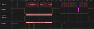
我暂时主要关注 SPI_READ 函数、我想如果可以的话、就能算出 SPI_WRITE

下面是我的尝试,它不起作用:

void Config_evm_spi(void)
{
//Pin Config
EALLOW;
// SPI_MOSI
GPIO_SetupPinOptions(16, GPIO_INPUT, GPIO_ASYNC | GPIO_PULLUP);
// SPI_MISO
GPIO_SetupPinOptions(17, GPIO_INPUT, GPIO_ASYNC | GPIO_PULLUP);
// SPI_CS
GPIO_SetupPinOptions(56, GPIO_INPUT, GPIO_ASYNC | GPIO_PULLUP);
// SPI_CLK
GPIO_SetupPinOptions(57, GPIO_INPUT, GPIO_ASYNC | GPIO_PULLUP);
GPIO_SetupPinMux(16, GPIO_MUX_CPU1, 1);
GPIO_SetupPinMux(17, GPIO_MUX_CPU1, 1);
GPIO_SetupPinMux(56, GPIO_MUX_CPU1, 1);
GPIO_SetupPinMux(57, GPIO_MUX_CPU1, 1);
EDIS;

EALLOW;
ClkCfgRegs.LOSPCP.all = 0;
EDIS;

// Initialize SPI FIFO registers
SpiaRegs.SPIFFTX.all = 0xE040;
SpiaRegs.SPIFFRX.all = 0x2044;
SpiaRegs.SPIFFCT.all = 0x0;

//SPI Settings
SpiaRegs.SPICCR.bit.SPISWRESET = 0;     //SPI Reset On
SpiaRegs.SPICCR.bit.CLKPOLARITY = 0;    //SCLK Active High
SpiaRegs.SPICCR.bit.SPICHAR = 0xF;      //16-bit SPI char
SpiaRegs.SPICCR.bit.SPILBK = 0;

SpiaRegs.SPICTL.bit.OVERRUNINTENA = 0;  //No overrun interrupt
SpiaRegs.SPICTL.bit.CLK_PHASE = 0;      //Phase 0
SpiaRegs.SPICTL.bit.MASTER_SLAVE = 1;   //Master mode
SpiaRegs.SPICTL.bit.TALK = 1;           //nSCS enabled
SpiaRegs.SPICTL.bit.SPIINTENA = 0;      //TX/RX Interrupt Disabled

SpiaRegs.SPIBRR.bit.SPI_BIT_RATE = ((25000000 / 1000000) - 1);              //Set baud rate to 1MHz
SpiaRegs.SPIPRI.bit.FREE = 1;           //Set so breakpoints don't disturb transmission
SpiaRegs.SPICCR.bit.SPISWRESET = 1;   //Exit SPI reset

}
Uint32 tspi_xmit(Uint32 spiFrame)
{
SpiaRegs.SPITXBUF = spiFrame;
//Wait for RX flag to indicate SPI frame completion
while(SpiaRegs.SPIFFRX.bit.RXFFST != 1)
{
}

return SpiaRegs.SPIRXBUF;

}
Uint32 tspi_read(Uint16 id, Uint16 addr)
{
Uint32 commandword = 0;
Uint16 data = 0; // No data to read
Uint16 p_addr = addr & 0x3F; // Ensure address is 6 bits (0-63)
// Construct the command word
commandword = (data & 0x7FFF) | (1 << 16) | (p_addr << 17); // 1 for read

// Calculate even parity for bits 0-15 and bits 16-23
Uint16 parity0 = 0, parity1 = 0;

int i;
for (i = 0; i < 16; i++) {
    parity0 ^= (commandword >> i) & 1;
}
for (i = 16; i < 24; i++) {
    parity1 ^= (commandword >> i) & 1;
}

// Set the parity bits
commandword |= (parity0 << 15) | (parity1 << 23);

return tspi_xmit(commandword);

}
Uint32 tspi_write(Uint16 id, Uint16 addr, Uint16 data)
{
Uint32 commandword = 0;
Uint16 p_addr = addr & 0x3F; // Ensure address is 6 bits (0-63)
// Construct the command word
commandword = (data & 0x7FFF) | (0 << 16) | (p_addr << 17); // 0 for write

// Calculate even parity for bits 0-15 and bits 16-23
Uint16 parity0 = 0, parity1 = 0;
int i;
for (i = 0; i < 16; i++) {
    parity0 ^= (commandword >> i) & 1;
}
for (i = 16; i < 24; i++) {
    parity1 ^= (commandword >> i) & 1;
}

// Set the parity bits
commandword |= (parity0 << 15) | (parity1 << 23);

return tspi_xmit(commandword);

}

谢谢!

Yara

  • 请注意,本文内容源自机器翻译,可能存在语法或其它翻译错误,仅供参考。如需获取准确内容,请参阅链接中的英语原文或自行翻译。

    您好、Yara、

    为了澄清一点、我们的 F28004x SPI 模块支持1至16个数据位的数据字长度。 我们本身不支持24位事务。 您能不能更高层次地解释一下您是如何尝试发送和接收24位数据的? 您 计划如何分解 24位数据、因为它将需要多个事务? 由于会有两个事务、 我想您 还应该背对背发送它们以确保芯片选择在整个期间保持低电平。 您现在是否运行代码? 是否发现特定错误? 抱歉回答所有问题-只是想了解这里的目标和您遇到的特定问题点。

    此外、您是否参考过 C2000Ware 中的 SPI 示例? ([C2000Ware]\driverlib\f28004x\examples\spi)

    此致、

    Allison

  • 请注意,本文内容源自机器翻译,可能存在语法或其它翻译错误,仅供参考。如需获取准确内容,请参阅链接中的英语原文或自行翻译。

    您好、Allison、

    感谢您确认  F28004x SPI 模块只能进行16位事务、一开始我想我遇到了这个问题、不过我怀疑就是这个问题。  

    至于如何发送接收24位数据、我认为最简单的方法是处理最左边的8位、然后是最右边的16位。

    我还有一些来自我们的某个具有32位 SPI 帧的器件的代码、如果可以的话? 我相信通过背靠背发送16位来处理它。

    Uint16 tspi_read(Uint16 id, Uint16 addr8)
    {
        Uint16 p_addr;
        Uint16 p_data;
        Uint16 left8;
        Uint16 right16;
    
        Uint16 addr6 = addr8 & 0x3F;
    
        Uint16 dummy = 0;
    
        p_addr = spi_parity_calc(addr6);
    
        left8 = (p_addr << 15) | (addr6 << 9) | (id << 8);
        SpiaRegs.SPITXBUF=left8;
    
    
        p_data = 0;
    
        right16 = 0x00;
        SpiaRegs.SPITXBUF= right16;
        while(SpiaRegs.SPIFFRX.bit.RXFFST != 2);
    
    
        //return SpiaRegs.SPIRXBUF;
        return spi_xmit((left8 << 15) | (right16));
    }
    
    Uint16 tspi_write(Uint16 id, Uint16 addr, Uint16 data)
    {
    
        Uint16 p_addr;
        Uint16 p_data;
        Uint16 commandword;
        Uint16 dummy;
    
        //16-bit header
        p_addr = spi_parity_calc(addr);
        commandword = (id << 11) | (addr << 3) | (p_addr << 0);
        SpiaRegs.SPITXBUF=commandword; //transmit header
        dummy = SpiaRegs.SPIRXBUF;
    
        //16 bit data
        p_data = spi_parity_calc(data);
        commandword = p_data | data;
        SpiaRegs.SPITXBUF=commandword; //transmit data
    
        while(SpiaRegs.SPIFFRX.bit.RXFFST != 2); //wait for 2 words to receive in FIFO
    
        return SpiaRegs.SPIRXBUF; //return last word
    }

    我的当前代码现在正在运行、但与器件的 SPI 通信已经基本实现

    谢谢

    Yara

  • 请注意,本文内容源自机器翻译,可能存在语法或其它翻译错误,仅供参考。如需获取准确内容,请参阅链接中的英语原文或自行翻译。

    您好、Yara、  

    到目前为止、运行代码是一个很好的开始-尽管存在 gibberish! 我们知道 GPIO 设置和连接已经建立。  

    我假设芯片选择需要在整个24或32位事务期间保持低电平、因此应确保 F28004x 发送两个 背对背传输以发送高位和低位、 然后在接收端重建数据 其他器件的器件型号是什么? 您是否确认全部满足了数据格式、时钟模式、芯片选择时序等要求? 如果设备不同意、这可能会破坏数据事务。

    您还可以使用内部环回模式(其中 TX 和 RX 在 F28004x 中内部连接在一起)来检查 SPI 是否成功独立于 DRV 器件运行。  

    此致、

    Allison

  • 请注意,本文内容源自机器翻译,可能存在语法或其它翻译错误,仅供参考。如需获取准确内容,请参阅链接中的英语原文或自行翻译。

    您好、Allsion:

    在24位事务期间、芯片选择确实需要保持低电平。

    [报价 userid="568270" url="~/support/microcontrollers/c2000-microcontrollers-group/c2000/f/c2000-microcontrollers-forum/1421059/launchxl-f280049c-converting-16-bit-spi-communication-code-to-24-bits/5447320 #5447320"]因此、您应确保 F28004x 发送两个 背靠背传输以发送高位和低位、 然后在接收端重构数据。[/QUOT]

    我认为这正是我真正陷入困境的地方、我不确定如何正确地解决这一问题。

    其他设备器件型号是什么? 您是否确认全部满足了数据格式、时钟模式、芯片选择时序等要求? 如果设备不同意、这可能会破坏数据事务。

    另一款使用32位 SPI 通信的器件是 DRV8311、其 SPI 时序要求与我正在开发的器件 DRV8376 24位 SPI 基本相同

    到目前为止我的代码看起来是这样的、我基于 DRV8311代码而不是 DRV8316  

    Uint32 tspi_read(Uint16 id, Uint16 addr)
    {
    Uint32 commandword = 0;
    Uint16 data = 0; // No data to read
    Uint16 p_addr = addr & 0x3F; // Ensure address is 6 bits (0-63)
    // Construct the command word
    commandword = (data & 0x7FFF) | (1 << 16) | (p_addr << 17); // 1 for read
    
    // Calculate even parity for bits 0-15 and bits 16-23
    Uint16 parity0 = 0, parity1 = 0;
    
    int i;
    for (i = 0; i < 16; i++) {
        parity0 ^= (commandword >> i) & 1;
    }
    for (i = 16; i < 24; i++) {
        parity1 ^= (commandword >> i) & 1;
    }
    
    // Set the parity bits
    commandword |= (parity0 << 15) | (parity1 << 23);
    
    return tspi_xmit(commandword);
    
    }
    Uint32 tspi_write(Uint16 id, Uint16 addr, Uint16 data)
    {
    Uint32 commandword = 0;
    Uint16 p_addr = addr & 0x3F; // Ensure address is 6 bits (0-63)
    // Construct the command word
    commandword = (data & 0x7FFF) | (0 << 16) | (p_addr << 17); // 0 for write
    
    // Calculate even parity for bits 0-15 and bits 16-23
    Uint16 parity0 = 0, parity1 = 0;
    int i;
    for (i = 0; i < 16; i++) {
        parity0 ^= (commandword >> i) & 1;
    }
    for (i = 16; i < 24; i++) {
        parity1 ^= (commandword >> i) & 1;
    }
    
    // Set the parity bits
    commandword |= (parity0 << 15) | (parity1 << 23);
    
    return tspi_xmit(commandword);
    
    }

    这是 SPI 事务的样子

    我不确定从哪里开始、好像一次只进行16位事务。

    谢谢!

    Yara

  • 请注意,本文内容源自机器翻译,可能存在语法或其它翻译错误,仅供参考。如需获取准确内容,请参阅链接中的英语原文或自行翻译。

    您好、Allison、

    我们会做些什么。

    我运行 DRV8311代码、感觉效果比调整后的代码更好

    Uint16 tspi_read(Uint16 id, Uint16 addr)
    {
        Uint16 p_addr;
        Uint16 p_data;
        Uint16 commandword;
    
        Uint16 dummy = 0xFF;
    
        p_addr = spi_parity_calc(addr);
        commandword = (0x8000) | (id << 11) | (addr << 3) | (p_addr << 0);
        SpiaRegs.SPITXBUF=commandword;
        dummy = SpiaRegs.SPIRXBUF;
    
        p_data = spi_parity_calc(dummy);
        commandword = (p_data << 15) | dummy;
        SpiaRegs.SPITXBUF=commandword;
        dummy = SpiaRegs.SPIRXBUF;
        while(SpiaRegs.SPIFFRX.bit.RXFFST != 2);
    
        dummy = SpiaRegs.SPIRXBUF;
        return SpiaRegs.SPIRXBUF;
    }
    
    Uint16 tspi_write(Uint16 id, Uint16 addr, Uint16 data)
    {
    
        Uint16 p_addr;
        Uint16 p_data;
        Uint16 commandword;
        Uint16 dummy;
    
        //16-bit header
        p_addr = spi_parity_calc(addr);
        commandword = (id << 11) | (addr << 3) | (p_addr << 0);
        SpiaRegs.SPITXBUF=commandword; //transmit header
        dummy = SpiaRegs.SPIRXBUF;
    
        //16 bit data
        p_data = spi_parity_calc(data);
        commandword = p_data | data;
        SpiaRegs.SPITXBUF=commandword; //transmit data
    
        while(SpiaRegs.SPIFFRX.bit.RXFFST != 2); //wait for 2 words to receive in FIFO
    
        return SpiaRegs.SPIRXBUF; //return last word
    }
    

  • 请注意,本文内容源自机器翻译,可能存在语法或其它翻译错误,仅供参考。如需获取准确内容,请参阅链接中的英语原文或自行翻译。

    您好、Yara、

    传输完成后、最佳做法是在读取之前检查 RXBUF 中是否有有效的完整数据。 此外、如果您始终接收24位数据、则可以使用8位 SPI 字符长度。 这样、您可以通过 TXFIFO 发送3次8位传输、并将全部3个 8位字符位接收到 RXFIFO 中。 您是否使用 FIFO 中断? 可以将 RXFFIL 设置为3、这样当您在 FIFO 中接收到三个字符时、将触发中断并可以重构24位数据-以下是伪代码:

    1. 发送3x8位数据
      • 注意事项:SPI FIFO 针对16位数据进行了优化 、因此在传输时、您写入 TXBUF 的数据应左对齐、因此在写入 TXBUF 以传输所需数据之前位移左<< 8。 由于器件向 RXBUF 的低位接收到数据、因此 RXBUF 中不需要此操作- TRM 中对此进行了介绍、但我想说一下。
    2. 等待 RXFIFO 深度显示3个 RX FIFO 深度已满数据。
      • 如果 RXFFIL 设置为3、这将触发 RX 中断(当 RXFIFO 中有3个或更多字时、中断被触发)
    3. 在 RX FIFO 中断中:
      • 从 RXBUF 读取3次来读取3x8位数据
      • 读取时、您可以将它们各保存到32位变量中(因为我们没有24位数据类型)、并相应地对数据进行位移、以便您可以或它们重建完整的数据。  

    如果要使用16位数据、仅需2次传输(RXFFIL 为2)、您可以对其进行调整、并必须调整移位以提取16位数据和8位数据。 您是否参考过任何具体的 C2000ware 示例? 我们有一些实现 FIFO 中断的协议、您可以参考这些协议。

    此致、  

    Allison

  • 请注意,本文内容源自机器翻译,可能存在语法或其它翻译错误,仅供参考。如需获取准确内容,请参阅链接中的英语原文或自行翻译。

    好的、我已经厌倦了实施你的建议、虽然我真的不熟悉 CCS、只使用我已经有的示例

    您是否已经参考过任何具体的 C2000ware 示例? 我们有一些实现 FIFO 中断的方法可以参考。[/QUOT]

    我一直使用先前团队成员编写的固件、所以他们可能已经引用了 C2000ware 示例?

    这是到目前为止我的 SPI 读写代码的样子

    Uint32 tspi_read(Uint16 id, Uint16 addr)
    {
    Uint16 p_addr, p_data;
    Uint32 commandword;
    Uint16 dummy = 0xFF;
    Uint32 received_data = 0;
    Uint8 byte1, byte2, byte3;
    // Calculate parity for the address
    p_addr = spi_parity_calc(addr);
    
    // Construct 24-bit command word:
    // Bit 23: Parity bit for bits 16-23 (addr parity)
    // Bits 17-22: Address
    // Bit 16: Read (1)
    // Bits 0-14: Empty, set to 0
    Uint8 tx_byte1 = 0x00;
    Uint8 tx_byte2 = (1 << 7);
    Uint8 tx_byte3 = (p_addr << 7) | ((addr & 0x3F) << 1);
    
    // Transmit command word (send as 3x 8-bit)
    SpiaRegs.SPITXBUF = tx_byte1;  // First 8 bits
    SpiaRegs.SPITXBUF = tx_byte2;  // Middle 8 bits
    SpiaRegs.SPITXBUF = tx_byte3;  // Last 8 bits
    
    // Wait for RXFIFO to be full (3x 8-bit data)
    while (SpiaRegs.SPIFFRX.bit.RXFFST < 3);
    
    // Read the received data (3x 8-bit)
    byte1 = SpiaRegs.SPIRXBUF & 0xFF;
    byte2 = SpiaRegs.SPIRXBUF & 0xFF;
    byte3 = SpiaRegs.SPIRXBUF & 0xFF;
    
    received_data = ((Uint32)byte1 <<16) | ((Uint32)byte2 << 8) | ((Uint32)byte3);
    
    return received_data;
    }
    
    
    Uint32 tspi_write(Uint16 id, Uint16 addr, Uint16 data)
    {
    Uint16 p_addr, p_data;
    Uint32 commandword;
    Uint32 received_data = 0;
    Uint8 byte1, byte2, byte3;
    // Calculate parity for address and data
    p_addr = spi_parity_calc(addr);
    p_data = spi_parity_calc(data);
    
    // Construct 24-bit command word:
    // Bit 23: Parity bit for bits 16-23 (addr parity)
    // Bits 17-22: Address
    // Bit 16: Write (0)
    // Bits 0-15: Data with parity bit
    Uint8 tx_byte1 = (p_data << 7) | ((data >> 8) & 0x7F);
    Uint8 tx_byte2 = data & 0xFF;
    Uint8 tx_byte3 = (p_addr << 7) | ((addr & 0x3F) << 1);
    
    
    // Transmit command word (send as 3x 8-bit)
    SpiaRegs.SPITXBUF = tx_byte1;  // First 8 bits
    SpiaRegs.SPITXBUF = tx_byte2;  // Middle 8 bits
    SpiaRegs.SPITXBUF = tx_byte3;  // Last 8 bits
    
    // Wait for RXFIFO to be full (3x 8-bit data)
    while (SpiaRegs.SPIFFRX.bit.RXFFST < 3);
    
    // Read the received data (3x 8-bit)
    byte1 = SpiaRegs.SPIRXBUF & 0xFF;
    byte2 = SpiaRegs.SPIRXBUF & 0xFF;
    byte3 = SpiaRegs.SPIRXBUF & 0xFF;
    
    received_data = ((Uint32)byte1 <<16) | ((Uint32)byte2 << 8) | ((Uint32)byte3);
    
    return received_data;
    }

    我不确定发生了什么、但当 ENABLE 为低电平时好像正在发生两个24位事务、所以我只需要弄清楚如何缩短 ENABLE 为低电平的时间、这样总结是正确的吗? 不确定在哪里或如何做到这一点?  

    ...

    在 Configure_EVM_SPI 函数中、我看到有一行提到 nSCS Enable

    此致、

    Yara

  • 请注意,本文内容源自机器翻译,可能存在语法或其它翻译错误,仅供参考。如需获取准确内容,请参阅链接中的英语原文或自行翻译。

    对不起所有的更新!

    我获得了24位交易、因此取得了一定的进展!

    Uint32 tspi_read(Uint16 id, Uint16 addr)
    {
    Uint16 p_addr, p_data;
    Uint32 commandword;
    Uint16 dummy = 0xFF;
    Uint32 received_data = 0;
    Uint8 byte1, byte2, byte3;
    // Calculate parity for the address
    p_addr = spi_parity_calc(addr & 0x3F);
    
    // Construct 24-bit:
    // Bit 23: Parity bit for bits 16-23 (addr parity)
    // Bits 17-22: Address
    // Bit 16: Read (1)
    // Bits 0-14: Empty, set to 0
    Uint8 tx_byte1 = (p_addr << 7) | ((addr & 0x3F) << 1) | 1;
    Uint8 tx_byte2 = 0;
    Uint8 tx_byte3 = 0;
    
    // Transmit command word (send as 3x 8-bit)
    SpiaRegs.SPITXBUF = tx_byte1;  // First 8 bits
    SpiaRegs.SPITXBUF = tx_byte2;  // Middle 8 bits
    SpiaRegs.SPITXBUF = tx_byte3;  // Last 8 bits
    
    // Wait for RXFIFO to be full (3x 8-bit data)
    while (SpiaRegs.SPIFFRX.bit.RXFFST < 3);
    
    // Read the received data (3x 8-bit)
    byte1 = SpiaRegs.SPIRXBUF & 0xFF;
    byte2 = SpiaRegs.SPIRXBUF & 0xFF;
    byte3 = SpiaRegs.SPIRXBUF & 0xFF;
    
    received_data = ((Uint32)byte1 <<16) | ((Uint32)byte2 << 8) | ((Uint32)byte3);
    
    return received_data;
    }
    
    
    Uint32 tspi_write(Uint16 id, Uint16 addr, Uint16 data)
    {
    Uint16 p_addr, p_data;
    Uint32 commandword;
    Uint32 received_data = 0;
    Uint8 byte1, byte2, byte3;
    // Calculate parity for address and data
    p_addr = spi_parity_calc(addr);
    p_data = spi_parity_calc(data);
    
    // Construct 24-bit command word:
    // Bit 23: Parity bit for bits 16-23 (addr parity)
    // Bits 17-22: Address
    // Bit 16: Write (0)
    // Bits 0-15: Data with parity bit
    Uint8 tx_byte1 = (p_addr << 7) | ((addr & 0x3F) << 1) | 0;
    Uint8 tx_byte2 = ((p_data << 7) | ((data >> 8) & 0x7F));
    Uint8 tx_byte3 = data & 0xFF;
    
    
    // Transmit command word (send as 3x 8-bit)
    SpiaRegs.SPITXBUF = tx_byte1;  // First 8 bits
    SpiaRegs.SPITXBUF = tx_byte2;  // Middle 8 bits
    SpiaRegs.SPITXBUF = tx_byte3;  // Last 8 bits
    
    // Wait for RXFIFO to be full (3x 8-bit data)
    while (SpiaRegs.SPIFFRX.bit.RXFFST < 3);
    
    // Read the received data (3x 8-bit)
    byte1 = SpiaRegs.SPIRXBUF & 0xFF;
    byte2 = SpiaRegs.SPIRXBUF & 0xFF;
    byte3 = SpiaRegs.SPIRXBUF & 0xFF;
    
    received_data = ((Uint32)byte1 <<16) | ((Uint32)byte2 << 8) | ((Uint32)byte3);
    
    return received_data;
    }
    

    现在、我遇到了所有事务基本上都是0的问题。 我想这可能是因为它和时序图不一样:

    我如何能够确保 SD/SDI 在 nSCS 变为低电平后等待一段时间?

    此致、

    Yara

  • 请注意,本文内容源自机器翻译,可能存在语法或其它翻译错误,仅供参考。如需获取准确内容,请参阅链接中的英语原文或自行翻译。

    您好、Yara、

    很高兴看到您获得24位交易! 如果出现零、这肯定是因为时间问题、或者可能是发送/接收机制。 上述代码片段是否适用于其他(非 C2000)器件? 在 C2000上、时钟线应该处于空闲低电平、在上升沿发送数据、在下降沿接收/锁存数据、这将是极性= 0、相位= 0。 假设您已经完成了该设置、那么您应该可以进行时钟模式。  不过、在上面发布的分析器屏幕截图中、当芯片选择为低电平时、MISO 和 MOSI 线路似乎在发送零。 这是故意的吗?

    隔离和测试 C2000 SPI 模块是否工作的一种方法是启用内部环回模式(这会在内部将 RX 和 TX 连接在一起以环回 SPI 数据)。 您是否可以尝试这样做、发送已知数据并检查您是否收到了相同的数据? 这将有助于了解 SPI 是否设置正确( 如果您只需查看 F28004x 器件即可更直观地了解是否正确发送和接收)。

    关于片选时序、此信息取决于 SPI 速度、并在我们的器件 数据表中进行了详细说明

    此致、

    Allison

  • 请注意,本文内容源自机器翻译,可能存在语法或其它翻译错误,仅供参考。如需获取准确内容,请参阅链接中的英语原文或自行翻译。

    您好、Allison、

    非常感谢您的支持!

    因此、我可以读取所有寄存器而不会出现任何问题、我的写函数也差不多可以正常工作了。 我遇到了一些时钟脉冲太长的问题? 导致 SPI 事务发生、因为它会触发多少个脉冲。

    为什么会发生这种情况、如何解决这种情况?

    让我的 SPI 事务真正起作用的另一件事是添加0x0000并将所需位进一步向左移动。 我很高兴它能起作用、但我真的不明白吗?

    此致、

    Yara

  • 请注意,本文内容源自机器翻译,可能存在语法或其它翻译错误,仅供参考。如需获取准确内容,请参阅链接中的英语原文或自行翻译。

    我的逻辑分析仪采样率太低、第一个问题已解决! 如果您能深入了解第二个问题、那就太好了。

  • 请注意,本文内容源自机器翻译,可能存在语法或其它翻译错误,仅供参考。如需获取准确内容,请参阅链接中的英语原文或自行翻译。

    您好、Yara、

    这是一个伟大的进步! 很高兴看到您可以运行它并解决采样率问题。 关于您的第二个问题、您将 TX_byte1初始化为0x0000是否存在某种原因? TX_BYTE1声明为8位变量、但看起来您正在超出8位、因此应该仅存储8个最低有效位、这可能会导致数据的高8位被切断。

    如果您记得我之前的注意事项、如果您正在传输8位数据、则应在写入 TXBUF 之前通过左移8位来左对齐。 这是预期结果吗? 是否尝试向 TXBUF 写入要传输的左对齐16位数据? P_addr 和 addr_READ 也是16位、这在我看来是合理的。 我的想法可能是、以前您没有正确左对齐的数据。

    此致、

    Allison