

Other Parts Discussed in Thread: C2000WARE,
HI,TI的工程师
我简单修改组合了TI的例程
C:\ti\C2000Ware_4_00_00_00\device_support\f2837xd\examples\cpu1\adc_soc_continuous
和
C:\ti\C2000Ware_4_00_00_00\device_support\f2837xd\examples\cpu1\epwm_up_aq,
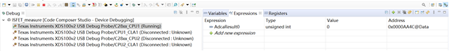
将PWM1A(launchpad标号40)连接到ADCINA0(launchpad标号30),测试LAUNCHXL-F28379D的ADC读取ePWM外设发出的信号,但watch窗口显示AdcaResult0值始终为0
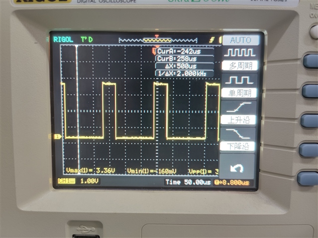
示波器测试ePWM输出波形正常
以下是我的代码,编译运行均无报错
//
// Included Files
//
#include "F28x_Project.h"

//
// Defines
//
#define EPWM1_TIMER_TBPRD  2000  // Period register
#define EPWM1_MIN_CMPA     500

//
// Globals
//
typedef struct
{
    volatile struct EPWM_REGS *EPwmRegHandle;
    Uint16 EPwmMinCMPA;
}EPWM_INFO;

EPWM_INFO epwm1_info;

Uint16 AdcaResult0;

//
//  Function Prototypes
//
void InitEPwm1Example(void);
void ConfigureADC(void);
void SetupADCSoftware(void);

//
// Main
//
void main(void)
{
//
// Step 1. Initialize System Control:
// PLL, WatchDog, enable Peripheral Clocks
// This example function is found in the F2837xD_SysCtrl.c file.
//
    InitSysCtrl();

//
// Step 2. Initialize GPIO:
// This example function is found in the F2837xD_Gpio.c file and
// illustrates how to set the GPIO to it's default state.
//
    InitGpio();

//
// Enable PWM1, PWM2 and PWM3
//
    CpuSysRegs.PCLKCR2.bit.EPWM1=1;

//
// For this case just init GPIO pins for ePWM1, ePWM2, ePWM3
// These functions are in the F2837xD_EPwm.c file
//
    InitEPwm1Gpio();

//
// Step 3. Clear all interrupts and initialize PIE vector table:
// Disable CPU interrupts
//
    DINT;

//
// Initialize the PIE control registers to their default state.
// The default state is all PIE interrupts disabled and flags
// are cleared.
// This function is found in the F2837xD_PieCtrl.c file.
//
    InitPieCtrl();

//
// Disable CPU interrupts and clear all CPU interrupt flags:
//
    IER = 0x0000;
    IFR = 0x0000;

//
// Initialize the PIE vector table with pointers to the shell Interrupt
// Service Routines (ISR).
// This will populate the entire table, even if the interrupt
// is not used in this example.  This is useful for debug purposes.
// The shell ISR routines are found in F2837xD_DefaultIsr.c.
// This function is found in F2837xD_PieVect.c.
//
    InitPieVectTable();


//
// For this example, only initialize the ePWM
//
    EALLOW;
    CpuSysRegs.PCLKCR0.bit.TBCLKSYNC = 0;
    EDIS;

    InitEPwm1Example();

    EALLOW;
    CpuSysRegs.PCLKCR0.bit.TBCLKSYNC = 1;
    EDIS;

//
// Step 4. User specific code, enable interrupts:
//
// Enable CPU INT3 which is connected to EPWM1-3 INT:
//
    IER |= M_INT3;

//
// Enable EPWM INTn in the PIE: Group 3 interrupt 1-3
//
    PieCtrlRegs.PIEIER3.bit.INTx1 = 1;

//
// Enable global Interrupts and higher priority real-time debug events:
//
    EINT;  // Enable Global interrupt INTM
    ERTM;  // Enable Global realtime interrupt DBGM

    //
    //Configure the ADCs and power them up
    //
        ConfigureADC();

    //
    //Setup the ADCs for software conversions
    //
        SetupADCSoftware();

    //
    //take conversions indefinitely in loop
    //
        do
        {
            //
            //convert, wait for completion, and store results
            //start conversions immediately via software, ADCA
            //
            AdcaRegs.ADCSOCFRC1.all = 0x0001; //SOC0

            //
            //wait for ADCA to complete, then acknowledge flag
            //
            while(AdcaRegs.ADCINTFLG.bit.ADCINT1 == 0);
            AdcaRegs.ADCINTFLGCLR.bit.ADCINT1 = 1;

            //
            //store results
            //
            AdcaResult0 = AdcaResultRegs.ADCRESULT0;

            //
            //at this point, conversion results are stored in
            //AdcaResult0, AdcaResult1, AdcbResult0, and AdcbResult1
            //

            //
            //software breakpoint, hit run again to get updated conversions
            //
            asm("   ESTOP0");

        }while(1);

}


//
// InitEPwm1Example - Initialize EPWM1 values
//
void InitEPwm1Example()
{
   //
   // Setup TBCLK
   //
   EPwm1Regs.TBCTL.bit.CTRMODE = TB_COUNT_UP; // Count up
   EPwm1Regs.TBPRD = EPWM1_TIMER_TBPRD;       // Set timer period
   EPwm1Regs.TBCTL.bit.PHSEN = TB_DISABLE;    // Disable phase loading
   EPwm1Regs.TBPHS.bit.TBPHS = 0x0000;        // Phase is 0
   EPwm1Regs.TBCTR = 0x0000;                  // Clear counter
   EPwm1Regs.TBCTL.bit.HSPCLKDIV = TB_DIV2;   // Clock ratio to SYSCLKOUT
   EPwm1Regs.TBCTL.bit.CLKDIV = TB_DIV2;

   //
   // Setup shadow register load on ZERO
   //
   EPwm1Regs.CMPCTL.bit.SHDWAMODE = CC_SHADOW;
   EPwm1Regs.CMPCTL.bit.LOADAMODE = CC_CTR_ZERO;

   //
   // Set Compare values
   //
   EPwm1Regs.CMPA.bit.CMPA = EPWM1_MIN_CMPA;     // Set compare A value

   //
   // Set actions
   //
   EPwm1Regs.AQCTLA.bit.ZRO = AQ_SET;            // Set PWM1A on Zero
   EPwm1Regs.AQCTLA.bit.CAU = AQ_CLEAR;          // Clear PWM1A on event A,
                                                 // up count

}

//
// ConfigureADC - Write ADC configurations and power up the ADC for both
//                ADC A and ADC B
//
void ConfigureADC(void)
{
    EALLOW;

    //
    //write configurations
    //
    AdcaRegs.ADCCTL2.bit.PRESCALE = 6; //set ADCCLK divider to /4
    AdcSetMode(ADC_ADCA, ADC_RESOLUTION_12BIT, ADC_SIGNALMODE_SINGLE);

    //
    //Set pulse positions to late
    //
    AdcaRegs.ADCCTL1.bit.INTPULSEPOS = 1;

    //
    //power up the ADCs
    //
    AdcaRegs.ADCCTL1.bit.ADCPWDNZ = 1;

    //
    //delay for 1ms to allow ADC time to power up
    //
    DELAY_US(1000);

    EDIS;
}

//
// SetupADCSoftware - Setup ADC channels and acquisition window
//
void SetupADCSoftware(void)
{
    Uint16 acqps;

    //
    //determine minimum acquisition window (in SYSCLKS) based on resolution
    //
        acqps = 14; //75ns

    //
    //Select the channels to convert and end of conversion flag
    //ADCA
    //
    EALLOW;
    AdcaRegs.ADCSOC0CTL.bit.CHSEL = 0;  //SOC0 will convert pin A0
    AdcaRegs.ADCSOC0CTL.bit.ACQPS = acqps; //sample window is acqps +
                                           //1 SYSCLK cycles
    AdcaRegs.ADCINTSEL1N2.bit.INT1SEL = 1; //end of SOC1 will set INT1 flag
    AdcaRegs.ADCINTSEL1N2.bit.INT1E = 1;   //enable INT1 flag
    AdcaRegs.ADCINTFLGCLR.bit.ADCINT1 = 1; //make sure INT1 flag is cleared
    EDIS;
}


//
// End of file
//
请问AdcaResult0无数据是什么原因呢?
谢谢!

