因为内存不够就把 28033_RAM_lnk.cmd修改了一下,结果DSP2803x_Headers_nonBIOS.cmd就报了这个错误:#10264 PARTID memory range。
28033_RAM_lnk.cmd文件如下。我主要是把RAML0L1改大了。
MEMORY
{
PAGE 0 :
/* BEGIN is used for the "boot to SARAM" bootloader mode */
BEGIN : origin = 0x000000, length = 0x000002
RAMM0 : origin = 0x000050, length = 0x0003B0
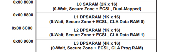
RAML0L1 : origin = 0x000800, length = 0x2F3F00
RESET : origin = 0x3FFFC0, length = 0x000002
IQTABLES : origin = 0x3FE000, length = 0x000B50 /* IQ Math Tables in Boot ROM */
IQTABLES2 : origin = 0x3FEB50, length = 0x00008C /* IQ Math Tables in Boot ROM */
IQTABLES3 : origin = 0x3FEBDC, length = 0x0000AA /* IQ Math Tables in Boot ROM */
BOOTROM : origin = 0x3FF27C, length = 0x000D44
PAGE 1 :
BOOT_RSVD : origin = 0x000002, length = 0x00004E /* Part of M0, BOOT rom will use this for stack */
RAMM1 : origin = 0x000480, length = 0x000380 /* on-chip RAM block M1 */
RAML2 : origin = 0x2F4700, length = 0x100450
RAML3 : origin = 0x3F4B50, length = 0x001000
}
SECTIONS
{
/* Setup for "boot to SARAM" mode:
The codestart section (found in DSP28_CodeStartBranch.asm)
re-directs execution to the start of user code. */
codestart : > BEGIN, PAGE = 0
ramfuncs : > RAMM0 PAGE = 0
.text : > RAML0L1, PAGE = 0
.cinit : > RAMM0, PAGE = 0
.pinit : > RAMM0, PAGE = 0
.switch : > RAMM0, PAGE = 0
.reset : > RESET, PAGE = 0, TYPE = DSECT /* not used, */
.stack : > RAMM1, PAGE = 1
.ebss : > RAML2, PAGE = 1
.econst : > RAML2, PAGE = 1
.esysmem : > RAML2, PAGE = 1
IQmath : > RAML0L1, PAGE = 0
IQmathTables : > IQTABLES, PAGE = 0, TYPE = NOLOAD
}
DSP2803x_Headers_nonBIOS.cmd我没有过。
MEMORY
{
 PAGE 0:    /* Program Memory */

 PAGE 1:    /* Data Memory */

   DEV_EMU     : origin = 0x000880, length = 0x000105     /* device emulation registers */
	 SYS_PWR_CTL : origin = 0x000985, length = 0x000003     /* System power control registers */
   FLASH_REGS  : origin = 0x000A80, length = 0x000060     /* FLASH registers */
   CSM         : origin = 0x000AE0, length = 0x000010     /* code security module registers */

   ADC_RESULT  : origin = 0x000B00, length = 0x000020     /* ADC Results register mirror */

   CPU_TIMER0  : origin = 0x000C00, length = 0x000008     /* CPU Timer0 registers */
   CPU_TIMER1  : origin = 0x000C08, length = 0x000008     /* CPU Timer0 registers (CPU Timer1 & Timer2 reserved TI use)*/
   CPU_TIMER2  : origin = 0x000C10, length = 0x000008     /* CPU Timer0 registers (CPU Timer1 & Timer2 reserved TI use)*/

   PIE_CTRL    : origin = 0x000CE0, length = 0x000020     /* PIE control registers */
   PIE_VECT    : origin = 0x000D00, length = 0x000100     /* PIE Vector Table */

   CLA1        : origin = 0x001400, length = 0x000080     /* CLA registers */

   ECANA       : origin = 0x006000, length = 0x000040     /* eCAN-A control and status registers */
   ECANA_LAM   : origin = 0x006040, length = 0x000040     /* eCAN-A local acceptance masks */
   ECANA_MOTS  : origin = 0x006080, length = 0x000040     /* eCAN-A message object time stamps */
   ECANA_MOTO  : origin = 0x0060C0, length = 0x000040     /* eCAN-A object time-out registers */
   ECANA_MBOX  : origin = 0x006100, length = 0x000100     /* eCAN-A mailboxes */

   COMP1       : origin = 0x006400, length = 0x000020     /* Comparator + DAC 1 registers */
   COMP2       : origin = 0x006420, length = 0x000020     /* Comparator + DAC 2 registers */
   COMP3       : origin = 0x006440, length = 0x000020     /* Comparator + DAC 3 registers */

   EPWM1       : origin = 0x006800, length = 0x000040     /* Enhanced PWM 1 registers */
   EPWM2       : origin = 0x006840, length = 0x000040     /* Enhanced PWM 2 registers */
   EPWM3       : origin = 0x006880, length = 0x000040     /* Enhanced PWM 3 registers */
   EPWM4       : origin = 0x0068C0, length = 0x000040     /* Enhanced PWM 4 registers */
   EPWM5       : origin = 0x006900, length = 0x000040     /* Enhanced PWM 5 registers */
   EPWM6       : origin = 0x006940, length = 0x000040     /* Enhanced PWM 6 registers */
   EPWM7       : origin = 0x006980, length = 0x000040     /* Enhanced PWM 7 registers */

   ECAP1       : origin = 0x006A00, length = 0x000020     /* Enhanced Capture 1 registers */

   HRCAP1      : origin = 0x006AC0, length = 0x000020     /* High Resolution Capture 1 registers */
   HRCAP2      : origin = 0x006AE0, length = 0x000020     /* High Resolution Capture 2 registers */

   EQEP1       : origin = 0x006B00, length = 0x000040     /* Enhanced QEP 1 registers */

   LINA        : origin = 0x006C00, length = 0x000080     /* LIN-A registers */

   GPIOCTRL    : origin = 0x006F80, length = 0x000040     /* GPIO control registers */
   GPIODAT     : origin = 0x006FC0, length = 0x000020     /* GPIO data registers */
   GPIOINT     : origin = 0x006FE0, length = 0x000020     /* GPIO interrupt/LPM registers */

   SYSTEM      : origin = 0x007010, length = 0x000020     /* System control registers */

   SPIA        : origin = 0x007040, length = 0x000010     /* SPI-A registers */
   SPIB        : origin = 0x007740, length = 0x000010     /* SPI-B registers */

   SCIA        : origin = 0x007050, length = 0x000010     /* SCI-A registers */

   NMIINTRUPT  : origin = 0x007060, length = 0x000010     /* NMI Watchdog Interrupt Registers */
   XINTRUPT    : origin = 0x007070, length = 0x000010     /* external interrupt registers */

   ADC         : origin = 0x007100, length = 0x000080     /* ADC registers */

   I2CA        : origin = 0x007900, length = 0x000040     /* I2C-A registers */

   PARTID      : origin = 0x3D7E80, length = 0x000001     /* Part ID register location */

   CSM_PWL     : origin = 0x3F7FF8, length = 0x000008     /* Part of FLASHA.  CSM password locations. */

}


SECTIONS
{
/*** PIE Vect Table and Boot ROM Variables Structures ***/
  UNION run = PIE_VECT, PAGE = 1
   {
      PieVectTableFile
      GROUP
      {
         EmuKeyVar
         EmuBModeVar
         FlashCallbackVar
         FlashScalingVar
      }
   }

/*** Peripheral Frame 0 Register Structures ***/
   DevEmuRegsFile    : > DEV_EMU,     PAGE = 1
	 SysPwrCtrlRegsFile: > SYS_PWR_CTL, PAGE = 1
   FlashRegsFile     : > FLASH_REGS,  PAGE = 1
   CsmRegsFile       : > CSM,         PAGE = 1
   AdcResultFile     : > ADC_RESULT,  PAGE = 1
   CpuTimer0RegsFile : > CPU_TIMER0,  PAGE = 1
   CpuTimer1RegsFile : > CPU_TIMER1,  PAGE = 1
   CpuTimer2RegsFile : > CPU_TIMER2,  PAGE = 1
   PieCtrlRegsFile   : > PIE_CTRL,    PAGE = 1
   Cla1RegsFile      : > CLA1,        PAGE = 1

/*** Peripheral Frame 1 Register Structures ***/
   ECanaRegsFile     : > ECANA,       PAGE = 1
   ECanaLAMRegsFile  : > ECANA_LAM,   PAGE = 1
   ECanaMboxesFile   : > ECANA_MBOX,  PAGE = 1
   ECanaMOTSRegsFile : > ECANA_MOTS,  PAGE = 1
   ECanaMOTORegsFile : > ECANA_MOTO,  PAGE = 1
   ECap1RegsFile     : > ECAP1,       PAGE = 1
   HRCap1RegsFile    : > HRCAP1,      PAGE = 1
   HRCap2RegsFile    : > HRCAP2,      PAGE = 1
   EQep1RegsFile     : > EQEP1,       PAGE = 1
   LinaRegsFile	     : > LINA,        PAGE = 1
   GpioCtrlRegsFile  : > GPIOCTRL,    PAGE = 1
   GpioDataRegsFile  : > GPIODAT,     PAGE = 1
   GpioIntRegsFile   : > GPIOINT,     PAGE = 1

/*** Peripheral Frame 2 Register Structures ***/
   SysCtrlRegsFile   : > SYSTEM,      PAGE = 1
   SpiaRegsFile      : > SPIA,        PAGE = 1
   SpibRegsFile      : > SPIB,        PAGE = 1
   SciaRegsFile      : > SCIA,        PAGE = 1
   NmiIntruptRegsFile: > NMIINTRUPT,  PAGE = 1
   XIntruptRegsFile  : > XINTRUPT,    PAGE = 1
   AdcRegsFile       : > ADC,         PAGE = 1
   I2caRegsFile      : > I2CA,        PAGE = 1

/*** Peripheral Frame 3 Register Structures ***/
   Comp1RegsFile     : > COMP1,    PAGE = 1
   Comp2RegsFile     : > COMP2,    PAGE = 1
   Comp3RegsFile     : > COMP3,    PAGE = 1
   EPwm1RegsFile     : > EPWM1,    PAGE = 1
   EPwm2RegsFile     : > EPWM2,    PAGE = 1
   EPwm3RegsFile     : > EPWM3,    PAGE = 1
   EPwm4RegsFile     : > EPWM4,    PAGE = 1
   EPwm5RegsFile     : > EPWM5,    PAGE = 1
   EPwm6RegsFile     : > EPWM6,    PAGE = 1
   EPwm7RegsFile     : > EPWM7,    PAGE = 1

/*** Code Security Module Register Structures ***/
   CsmPwlFile        : > CSM_PWL,  PAGE = 1

/*** Device Part ID Register Structures ***/
   PartIdRegsFile    : > PARTID,   PAGE = 1

}
请大家帮我看一下,谢谢!