Part Number: MSP430AFE253
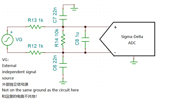
Many documents mention that using a SD ADC requires adding an anti-aliasing RC circuit as its front-end for differential inputs, as shown in the first figure below. Actual tests on the MSP430AFE's SD24_A achieved a sampling ripple as low as 0.03mV (using a sampling rate fS = fM / OSR = 60Hz, along with a software-implemented 10Hz low-pass filter).
However, the ADC itself has a certain input impedance, and the resistors in the front-end circuit can affect sampling accuracy. Moreover, my external signal source also has some output impedance (at least 50KΩ). As a result, the currently measured voltage values are inaccurate (though the calculations are correct). Therefore, I'm considering adding an op-amp buffer circuit at the front. Between the two options below, which is better?
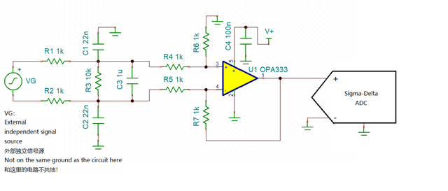
In the second figure, the signal first passes through the anti-aliasing RC circuit, then through a differential op-amp circuit before reaching the ADC. This seems feasible, but could there be an issue since the anti-aliasing RC circuit is not directly connected to the ADC input?
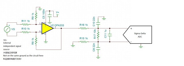
In the third figure, to address the concern above, the positions of the anti-aliasing RC circuit and the op-amp circuit are swapped. Would this be better? However, this introduces a new problem: my input signal is generated by an external independent circuit, which does not share a common ground with this ADC circuit. Is it acceptable to directly connect this output signal to the differential op-amp?