This thread has been locked.

If you have a related question, please click the "Ask a related question" button in the top right corner. The newly created question will be automatically linked to this question.

MSP430AFE253: Sigma-Delta ADC的前端电路设计哪一个更优?

Part Number: MSP430AFE253
Other Parts Discussed in Thread: TINA-TI

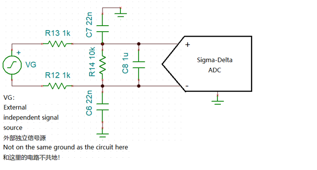
很多文档提到,使用 SD ADC 需要对其 差分输入 增加 抗混叠 RC 电路当作其前端电路,如下第一个图,实测在 MSP430AFE 的 SD24_A 上得到了 达到 0.03mV 的采集纹波(使用采样率 fS = fM / OSR = 60Hz,并加上软件实现的 10Hz 低通滤波) 。
但是ADC具有一定输入阻抗,而前端电路存在的电阻会对采集精度造成影响,况且我的外部信号源也存在一定的输出阻抗(至少50KΩ),所以实测现在采集的电压量不准(计算是没有问题的),所以想在前面增加运放电路在缓冲下,如下两种,哪一种更优?
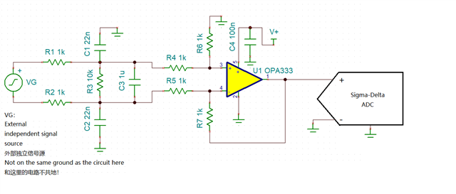
第二张图片,信号输入先经过抗混叠RC电路再经过差分运放电路再给到ADC,看起来可以,但是ADC输入的前面没有首先连接抗混叠RC电路是否会有问题?
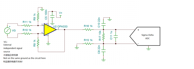
第三张图片,基于第二张图的疑惑,把抗混叠RC电路和运放电路交换位置,是否更好?但是有引入新的问题,我的输入信号是外部独立电路产生的输出信号,与这个ADC电路并不共地,这个输出信号直接连接差分运放是否可行?

Many documents mention that using a SD ADC requires adding an anti-aliasing RC circuit as its front-end for differential inputs, as shown in the first figure below. Actual tests on the MSP430AFE's SD24_A achieved a sampling ripple as low as 0.03mV (using a sampling rate fS = fM / OSR = 60Hz, along with a software-implemented 10Hz low-pass filter).

However, the ADC itself has a certain input impedance, and the resistors in the front-end circuit can affect sampling accuracy. Moreover, my external signal source also has some output impedance (at least 50KΩ). As a result, the currently measured voltage values are inaccurate (though the calculations are correct). Therefore, I'm considering adding an op-amp buffer circuit at the front. Between the two options below, which is better?

In the second figure, the signal first passes through the anti-aliasing RC circuit, then through a differential op-amp circuit before reaching the ADC. This seems feasible, but could there be an issue since the anti-aliasing RC circuit is not directly connected to the ADC input?

In the third figure, to address the concern above, the positions of the anti-aliasing RC circuit and the op-amp circuit are swapped. Would this be better? However, this introduces a new problem: my input signal is generated by an external independent circuit, which does not share a common ground with this ADC circuit. Is it acceptable to directly connect this output signal to the differential op-amp?

  • 您好

    已经收到了您的案例,调查需要些时间,感谢您的耐心等待

  • 另外,这种把运放接成差分电路的方式,会对运放的输入阻抗、CMRR有很大影响,因此进一步的,考虑使用仪表放大器或者全差分放大器,有哪些推荐吗,要求Vos远小于0.1mV,Ibias等参数,根据上述描述的场景,推荐一些合适的芯片型号,以及参考电路,适用于上述的场景。
    Additionally, configuring the op-amp as a differential circuit significantly impacts its input impedance and CMRR. Therefore, it’s worth considering instrumentation amplifiers or fully differential amplifiers. Do you have any recommendations? The requirements include a Vos well below 0.1mV and specifications like Ibias. Based on the described scenario, could you suggest suitable chip models and reference circuits tailored for this application?

  • 备忘:那两个运放缓冲的abc前端电路,我有空在 TINA-TI 上再用实际adc芯片仿真一下,输入端用一个电池电源(独立地)再加一点噪声。

  • We recommend only use RC without OPA in this condition. Because sigma-delta ADC should be calibrated by software for precise measure whether OPA is used or not. In the case software calibration is a must-have process, I think OPA is not necessary.

  • 我的信号源是一个TIA电路运放输出带50K的RC,我再串联一个10K电阻做分压,分压后的信号用于ADC测量(因为MSP430AFE的输入范围是0.5V因此我得用电阻分压,信号源电路我不能改动),ADC有输入电阻,因此可能造成静态误差,这个我可以接受,问题是,这个ADC采集的时候会不会对信号造成扰动(扰动机制:在每个调制器采样相的开关闭合瞬间,ADC会从输入源汲取一个大的瞬态电流脉冲,以对C_s充电/放电。这会导致分压点电压产生一个瞬间跌落/抬升(glitch)),这个动态误差就没准了,你推荐只使用RC而不用加运放环节进行缓冲,我再确认一下,你是确定推荐这么做吗?这个ADC对这个情况的电路采集的时候,动态误差和扰动是怎么样的?

    My signal source consists of an op-amp output followed by a 50K RC,  and I put a 10K resistor to gnd to it for voltage divider, with the divided signal fed into an ADC (since the MSP430AFE’s input range is 0.5V, I have to use the divider—the signal source circuit cannot be modified). The ADC has an input resistance, which may introduce static error, but I can tolerate that.

    My main concern is whether the ADC sampling process will disturb the signal.

    • Disturbance mechanism: During each modulator sampling phase (when the switch closes), the ADC draws a large transient current pulse from the input source to charge/discharge the sampling capacitor (C_s). This causes a voltage glitch (instantaneous dip/spike) at the divider node.

    • This dynamic error is unpredictable.

    You recommended using only an RC network without adding an op-amp buffer.

    • I want to confirm: Are you certain this approach is advisable?

    • For this specific circuit configuration, what level of dynamic error and signal disturbance should I expect during ADC sampling?


  • any reply here?