Part Number: BQ25756
The issue is as described in the subject line:
1、The design parameters are as follows: the input source is 57–60 V, and the charging output is 56 V / 2 A. The ACUV pin is measured at 7.4 V and the ACOV pin at 3.4 V, which meet the operating conditions.
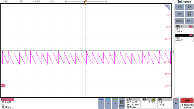
2、An external 12 V is supplied to the DRV_SUP pin, but it was confirmed that there is no voltage output at the REGN pin.
3、The /CE pin is connected to ground in the circuit, and the EN_CHG bit in the register is enabled, but there is still no output.
4、The I²C communication is functioning properly.
The schematic and register configuration parameters are attached. Could you please help advise how I can troubleshoot the issue?
* Created: Mon Oct 13 16:27:56 CST 2025
*
* Format: Register Name  tab Character,\t  Register Address  tab Character,\t  Hexadecimal register value.
* Device: BQ25756
* BQZ Container: Charger_1_00-bq25756.bqz
*
Charge Voltage Limit	0008
Charge Current Limit	00A0
Output Voltage Limit	0000
Input Current DPM Limit	0640
Input Voltage DPM Limit	0348
Reverse Mode Input Current Limit	0640
Reverse Mode Input Voltage Limit	03E8
Precharge Current Limit	0050
Termination Current Limit	0028
Precharge and Termination Control	0F
Timer Control	0D
Charger Control	C9
Pin Control	C0
Power Path and Reverse Mode Control	20
MPPT Control	20
TS Charging Threshold Control	96
TS Charging Region Behavior Control	57
TS Reverse Mode Threshold Control	40
Reverse Undervoltage Control	00
VAC Max Power Point Detected	0000
Charger Status 1	03
Charger Status 2	00
Charger Status 3	02
Fault Status	40
Charger Flag 1	00
Charger Flag 2	00
Fault Flag	00
Charger Mask 1	00
Charger Mask 2	00
Fault Mask	00
ADC Control	60
ADC Channel Control	02
IAC ADC - Use Field View	0000
IBAT ADC - Use Field View	0000
VAC ADC	0000
VBAT ADC	0000
TS ADC	0000
VFB ADC	0000
Gate Driver Strength Control	00
Gate Driver Dead Time Control	00
Part Information	12
Reverse Mode Battery Discharge Current	02