If you have a related question, please click the "Ask a related question" button in the top right corner. The newly created question will be automatically linked to this question.
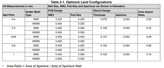
We have a number of app noted that can be referenced. The PCB pad size, PCB solder mask opening size, and stencil thickness guidelines provided by TI are meant to be a good starting point.
There are many variables that come into play which may require these parameters to be adjusted. For example, some PCBs may warp during reflow worse than other PCBs, which requires more solder paste volume to be deposited to achieve reliable connectivity. The solder paste volume required to achieve good connective can also vary from one type of solder paste to another type of solder paste. The thickness of the stencil and shape of the apertures may need to be adjusted to deposit an appropriate volume of solder paste on the PCB. The PCB assembly vendor may need to perform many trial runs adjusting these parameters until they develop a reliable recipe the specific combination of PCB and components being installed on the PCB.
Below is one of the app note link and the required info captured.
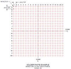
When we design the PCB land pad and stencil, we will look at the substrate pad size, solder ball dimension and ball pitch to come up the optimized design to obtain a good solder joint.
This will be validated by running BLR (Board level reliability) to look at the joint reliability.
Reducing the stencil thickness will reduce the total solder paste volume affecting the final joint shape and standoff. Increasing the stencil aperture to compensate the volume may not work since the paste pattern will be different so as the final joint shape.
If a customer want to reduce the stencil thickness because of other Components on their board, then I would suggest them to consider using a step up stencil (different stencil thickness at different location).