Hi Sir,
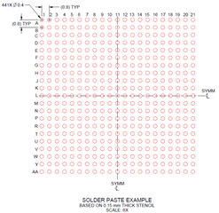
這顆料平面度到0.15mm,TI 規格書建議開0.15mm鋼板;高於目前加工廠常用的0.1mm, 0.12mm厚度,有一定的風險空焊, 會造成後端生產上的問題。
請問有辦法達到平面度0.1mm嗎?


BR,
Taylor
This thread has been locked.
If you have a related question, please click the "Ask a related question" button in the top right corner. The newly created question will be automatically linked to this question.
Hi Sir,
這顆料平面度到0.15mm,TI 規格書建議開0.15mm鋼板;高於目前加工廠常用的0.1mm, 0.12mm厚度,有一定的風險空焊, 會造成後端生產上的問題。
請問有辦法達到平面度0.1mm嗎?


BR,
Taylor
这个问题我需要咨询一下e2e论坛上的产品线工程确认,请关注下面帖子的回复。
https://e2e.ti.com/support/processors-group/processors/f/processors-forum/1177560/am6412-can-the-thick-stencil-be-changed-to-0-1mm
请看下面我们e2e工程师的回复。
The amount of the paste is dependent on the stencil thickness.
The .127 thickness would be a possibility if customer can make some changes to ensure that the solder paste to solder the ball is available.
I will check internally and update you on the feasibility.
请看下面我们e2e工程师最新的回复。
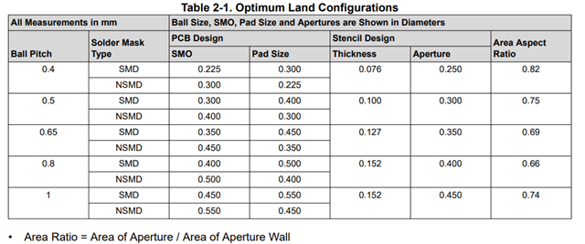
We have a number of app noted that can be referenced. The PCB pad size, PCB solder mask opening size, and stencil thickness guidelines provided by TI are meant to be a good starting point.
There are many variables that come into play which may require these parameters to be adjusted. For example, some PCBs may warp during reflow worse than other PCBs, which requires more solder paste volume to be deposited to achieve reliable connectivity. The solder paste volume required to achieve good connective can also vary from one type of solder paste to another type of solder paste. The thickness of the stencil and shape of the apertures may need to be adjusted to deposit an appropriate volume of solder paste on the PCB. The PCB assembly vendor may need to perform many trial runs adjusting these parameters until they develop a reliable recipe the specific combination of PCB and components being installed on the PCB.
Below is one of the app note link and the required info captured.
https://www.ti.com/lit/an/spraa99c/spraa99c.pdf
Here are the additional inputs i received
When we design the PCB land pad and stencil, we will look at the substrate pad size, solder ball dimension and ball pitch to come up the optimized design to obtain a good solder joint.
This will be validated by running BLR (Board level reliability) to look at the joint reliability.
Reducing the stencil thickness will reduce the total solder paste volume affecting the final joint shape and standoff. Increasing
the stencil aperture to compensate the volume may not work since the paste pattern will be different so as the final joint shape.
If a customer want to reduce the stencil thickness because of other Components on their board, then I would suggest them to consider
using a step up stencil (different stencil thickness at different location).