Part Number: TMS320F28035
Other Parts Discussed in Thread: C2000WARE, CONTROLSUITE
新手一枚,想请大神看一下我的adc采样配置有没有问题。代码已上传:
#include "DSP28x_Project.h"     // Device Headerfile and Examples Include File

// Prototype statements for functions found within this file.
__interrupt void adc_isr(void);
void Adc_Config(void);


// Global variables used in this example:
Uint16 LoopCount;
Uint16 ConversionCount;
Uint16 Voltage1[10];
Uint16 Voltage2[10];
Uint16 Voltage3[10];
Uint16 Voltage4[10];


main()
{

// Step 1. Initialize System Control:
// PLL, WatchDog, enable Peripheral Clocks
// This example function is found in the DSP2803x_SysCtrl.c file.
   InitSysCtrl();


// Step 2. Initialize GPIO:
// This example function is found in the DSP2803x_Gpio.c file and
// illustrates how to set the GPIO to it's default state.
// InitGpio();  // Skipped for this example

// Step 3. Clear all interrupts and initialize PIE vector table:
// Disable CPU interrupts
   DINT;

// Initialize the PIE control registers to their default state.
// The default state is all PIE interrupts disabled and flags
// are cleared.
// This function is found in the DSP2803x_PieCtrl.c file.
   InitPieCtrl();

// Disable CPU interrupts and clear all CPU interrupt flags:
   IER = 0x0000;
   IFR = 0x0000;

// Initialize the PIE vector table with pointers to the shell Interrupt
// Service Routines (ISR).
// This will populate the entire table, even if the interrupt
// is not used in this example.  This is useful for debug purposes.
// The shell ISR routines are found in DSP2803x_DefaultIsr.c.
// This function is found in DSP2803x_PieVect.c.
   InitPieVectTable();

// Interrupts that are used in this example are re-mapped to
// ISR functions found within this file.
   EALLOW;  // This is needed to write to EALLOW protected register
   PieVectTable.ADCINT1 = &adc_isr;
   EDIS;    // This is needed to disable write to EALLOW protected registers

// Step 4. Initialize all the Device Peripherals:
// This function is found in DSP2803x_InitPeripherals.c
// InitPeripherals(); // Not required for this example
   InitAdc();  // For this example, init the ADC

// Step 5. User specific code, enable interrupts:

// Enable ADCINT1 in PIE
   PieCtrlRegs.PIEIER1.bit.INTx1 = 1;   // Enable INT 1.1 in the PIE
   IER |= M_INT1;                       // Enable CPU Interrupt 1
   EINT;                                // Enable Global interrupt INTM
   ERTM;                                // Enable Global realtime interrupt DBGM

   LoopCount = 0;
   ConversionCount = 0;

// Configure ADC
// Note: Channel ADCINA4  will be double sampled to workaround the ADC 1st sample issue for rev0 silicon errata

    EALLOW;
    AdcRegs.ADCCTL1.bit.INTPULSEPOS = 1;    //ADCINT1 trips after AdcResults latch
    AdcRegs.INTSEL1N2.bit.INT1E     = 1;    //Enabled ADCINT1
    AdcRegs.INTSEL1N2.bit.INT1CONT  = 0;    //Disable ADCINT1 Continuous mode
    AdcRegs.INTSEL1N2.bit.INT1SEL   = 2;    //setup EOC2 to trigger ADCINT1 to fire

    AdcRegs.ADCSOC0CTL.bit.CHSEL    = 1;    //set SOC0 channel select to ADCINA1(dummy sample for rev0 errata workaround)
    AdcRegs.ADCSOC1CTL.bit.CHSEL    = 1;    //set SOC1 channel select to ADCINA1
    AdcRegs.ADCSOC2CTL.bit.CHSEL    = 2;    //set SOC2 channel select to ADCINA2
    AdcRegs.ADCSOC3CTL.bit.CHSEL    = 4;    //set SOC3 channel select to ADCINA4
    AdcRegs.ADCSOC4CTL.bit.CHSEL    = 6;    //set SOC4 channel select to ADCINA6

    AdcRegs.ADCSOC0CTL.bit.TRIGSEL  = 9;    //set SOC0 start trigger on EPwm3A, due to round-robin SOC0 converts first then SOC1, then SOC2
    AdcRegs.ADCSOC1CTL.bit.TRIGSEL  = 9;    //set SOC1 start trigger on EPwm3A, due to round-robin SOC0 converts first then SOC1, then SOC2
    AdcRegs.ADCSOC2CTL.bit.TRIGSEL  = 9;    //set SOC2 start trigger on EPwm3A, due to round-robin SOC0 converts first then SOC1, then SOC2
    AdcRegs.ADCSOC3CTL.bit.TRIGSEL  = 9;    //set SOC1 start trigger on EPwm3A, due to round-robin SOC0 converts first then SOC1, then SOC2
    AdcRegs.ADCSOC4CTL.bit.TRIGSEL  = 9;    //set SOC2 start trigger on EPwm3A, due to round-robin SOC0 converts first then SOC1, then SOC2

    AdcRegs.ADCSOC0CTL.bit.ACQPS    = 9;    //set SOC0 S/H Window to 7 ADC Clock Cycles, (9 ACQPS plus 1)
    AdcRegs.ADCSOC1CTL.bit.ACQPS    = 9;    //set SOC1 S/H Window to 7 ADC Clock Cycles, (9 ACQPS plus 1)
    AdcRegs.ADCSOC2CTL.bit.ACQPS    = 9;    //set SOC2 S/H Window to 7 ADC Clock Cycles, (9 ACQPS plus 1)
    AdcRegs.ADCSOC3CTL.bit.ACQPS    = 9;    //set SOC1 S/H Window to 7 ADC Clock Cycles, (9 ACQPS plus 1)
    AdcRegs.ADCSOC4CTL.bit.ACQPS    = 9;    //set SOC2 S/H Window to 7 ADC Clock Cycles, (9 ACQPS plus 1)
    EDIS;

// Assumes EPwm3 clock is already enabled in InitSysCtrl();
   EPwm3Regs.ETSEL.bit.SOCAEN   = 1;        // Enable SOC on A group
   EPwm3Regs.ETSEL.bit.SOCASEL  = 4;        // Select SOC from from CPMA on upcount
   EPwm3Regs.ETPS.bit.SOCAPRD   = 1;        // Generate pulse on 1st event
   EPwm3Regs.CMPA.half.CMPA     = 0x0080;   // Set compare A value
   EPwm3Regs.TBPRD              = 0xFFFF;   // Set period for EPwm3
   EPwm3Regs.TBCTL.bit.CTRMODE  = 0;        // count up and start

// Wait for ADC interrupt
   for(;;)
   {
      LoopCount++;
   }

}

__interrupt void  adc_isr(void)
{

  Voltage1[ConversionCount] = AdcResult.ADCRESULT1; //discard ADCRESULT0 as part of the workaround to the 1st sample errata for rev0
  Voltage2[ConversionCount] = AdcResult.ADCRESULT2;
  Voltage3[ConversionCount] = AdcResult.ADCRESULT3;
  Voltage4[ConversionCount] = AdcResult.ADCRESULT4;

  // If 20 conversions have been logged, start over
  if(ConversionCount == 9)
  {
     ConversionCount = 0;
  }
  else ConversionCount++;

  AdcRegs.ADCINTFLGCLR.bit.ADCINT1 = 1;     //Clear ADCINT1 flag reinitialize for next SOC
  PieCtrlRegs.PIEACK.all = PIEACK_GROUP1;   // Acknowledge interrupt to PIE

  return;
}
其中关于adc的设置有疑问的点在于:
Voltage1[ConversionCount] = AdcResult.ADCRESULT1;
Voltage2[ConversionCount] = AdcResult.ADCRESULT2;
Voltage3[ConversionCount] = AdcResult.ADCRESULT3;
Voltage4[ConversionCount] = AdcResult.ADCRESULT4;
这几行代码里的ADCRESULT1至ADCRESULT4的数字1至4是怎么来的。
//***************************************************************************************************
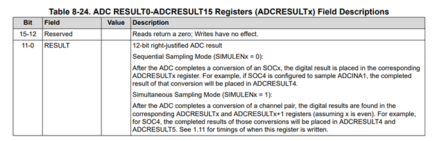
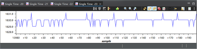
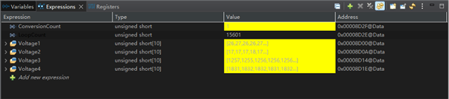
下面附上程序刷进F28035后,调试时voltage1至voltag4的采样截图和Expressions截图:
voltage1:
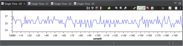
voltage2:
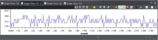
voltage3:
voltage4:
Expressions:
问题是:
1.我的adc配置是否有问题。
2.为什么voltage1和voltage2的数值分别在25和17上下浮动,而voltage3和voltage4的数值分别在1255和1830上下浮动。
3.为什么每组adc采样的voltage数值浮动范围都不一样,到底voltage的数值应该是多少。