

Part Number: TMS320F280033
手册zhcuao0b Page12 中提到
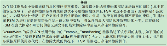
示例代码如下:
u32CurrentAddress = Bzero_Sector8_start;
oReturnCheck = Fapi_issueBankEraseCommand((uint32 *)u32CurrentAddress, 0x001F);
// Wait until FSM is done with bank erase operation
while (Fapi_checkFsmForReady() != Fapi_Status_FsmReady)
{
//
// Initialize the Erase Pulses to zero after issuing max pulses
//
if(HWREG(FLASH0CTRL_BASE + FLASH_O_ACC_EP) > MAX_ERASE_PULSE)
{
EALLOW;
//
// Enable Flash Optimization
//
HWREG(FLASH0CTRL_BASE + FLASH_O_OPT) = OPT_ENABLE;
HWREG(FLASH0CTRL_BASE + FLASH_O_ERA_PUL) =
HWREG(FLASH0CTRL_BASE + FLASH_O_ERA_PUL) &
~(uint32_t)FLASH_ERA_PUL_MAX_ERA_PUL_M;
//
// Disable Flash Optimization
//
HWREG(FLASH0CTRL_BASE + FLASH_O_OPT) = OPT_DISABLE;
EDIS;
}
}
代码中使用driverlib模式操作寄存器。
其中用到的几个宏定义如下(位于文件flash_programming_f28003x.h中):
#define FLASH0CTRL_BASE           0x0005F800U
#define FLASH0ECC_BASE            0x0005FB00U

//
// FMC Registers, Masks and Values
//
#define FLASH_O_ACC_EP           0x148U    // Flash Accumulated Erase Pulses
#define FLASH_O_ERA_PUL          0x136U    // Flash Max Erase Pulses
#define FLASH_O_OPT              0x144U    // Flash Optimization

#define FLASH_ERA_PUL_MAX_ERA_PUL_M      0xFFFU  // Flash Max Erase Pulses Mask
#define OPT_ENABLE                       0x5U    // Flash Optimization Enable
#define OPT_DISABLE                      0x2U    // Flash Optimization Disable
#define MAX_ERASE_PULSE                  0x7D0U  // Flash Max Erase Pulses
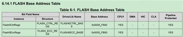
在28003x参考手册sprui33f 中FLASH0_CTRL_REGS定义如下:
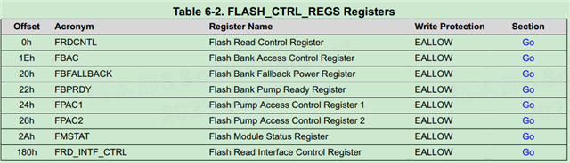
参考手册中并没有偏移地址为以下几个地址的寄存器说明:
0x148U // Flash Accumulated Erase Pulses
0x136U // Flash Max Erase Pulses
0x144U // Flash Optimization
请问那里可以看到这几个寄存器的具体定义以及说明?
如果不使用driverlib,如何定义这些寄存器呢?(的f28003x_flash.h中没有定义这几个寄存器)
struct FLASH_CTRL_REGS {
    union   FRDCNTL_REG                      FRDCNTL;                      // Flash Read Control Register
    Uint16                                   rsvd1[28];                    // Reserved
    union   FBAC_REG                         FBAC;                         // Flash Bank Access Control Register
    union   FBFALLBACK_REG                   FBFALLBACK;                   // Flash Bank Fallback Power Register
    union   FBPRDY_REG                       FBPRDY;                       // Flash Bank Pump Ready Register
    union   FPAC1_REG                        FPAC1;                        // Flash Pump Access Control Register 1
    union   FPAC2_REG                        FPAC2;                        // Flash Pump Access Control Register 2
    Uint16                                   rsvd2[2];                     // Reserved
    union   FMSTAT_REG                       FMSTAT;                       // Flash Module Status Register
    Uint16                                   rsvd3[340];                   // Reserved
    union   FRD_INTF_CTRL_REG                FRD_INTF_CTRL;                // Flash Read Interface Control Register
};
