


hi TI experts:
我目前使用关于TCI6636(K2H)的DDR3B接口,芯片上DDR3A接的是IS43TR16512A-125KBLI型号4G的芯片,DDR3B接的是MT41K256M16TW-107,大小为2G的内存。均64bit连接,没有ECC。目前DDR3A可以访问0x80000000,而且DSP利用map寄存器也可以访问另外4G的内容。但是DDR3B目前我无法正常访问,配置好DDR3B后,CCS6一访问内存0x60000000的地址IDE环境就挂掉了。
根据TI的SPRS835F手册,DDR3B的地址在0x60000000可以访问,我目前硬件 DDR3A_REMAP_EN=1。想请高手帮着看看是DDR3B哪里配置不正确。根据配置流程,进行leveling,但是在执行leveling后,没有完全正确。
我参考sprabx7文档中DDR3的流程,有leveling的错误log。目前DDR3B的phy的配置是根据(TI6636 K2H KeystoneII关于DDR3初始化的配置.xlsx)来配置的。 目前硬件测试了时钟,是666MHz,波形良好,片选上有信号,DDR3B上电压是1.5V。DDR3B执行leveling之前DDR3B_PGSR0 = 0xB00001FF,执行leveling之后是DDR3B_PGSR0 = 0xB1C001FF,可以看附件里的DDR3A和DDR3B的gel的log(我尝试修改了phy的配置,最终现象一致,还是RDERR has ERROE)。
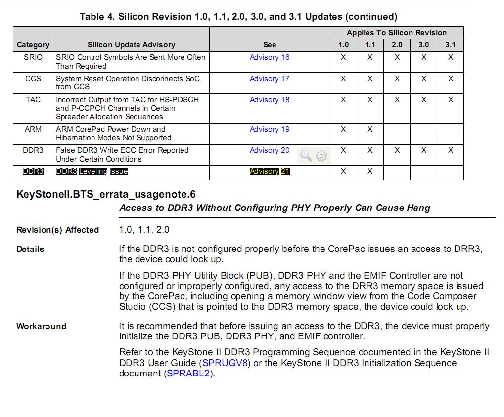
我从勘误表中找到的,目前我芯片使用的版本是CPU: 66AK2Hx SR2.0, 其中Advisory21应该针对2.0不受影响,目前遇到的问题类似KeyStoneII.BTS_errata_usagenote.6,我按照手册以及xls的配置,不知道Phy配置是否合适。想咨询下,看能否提供一些支持或者建议。
。
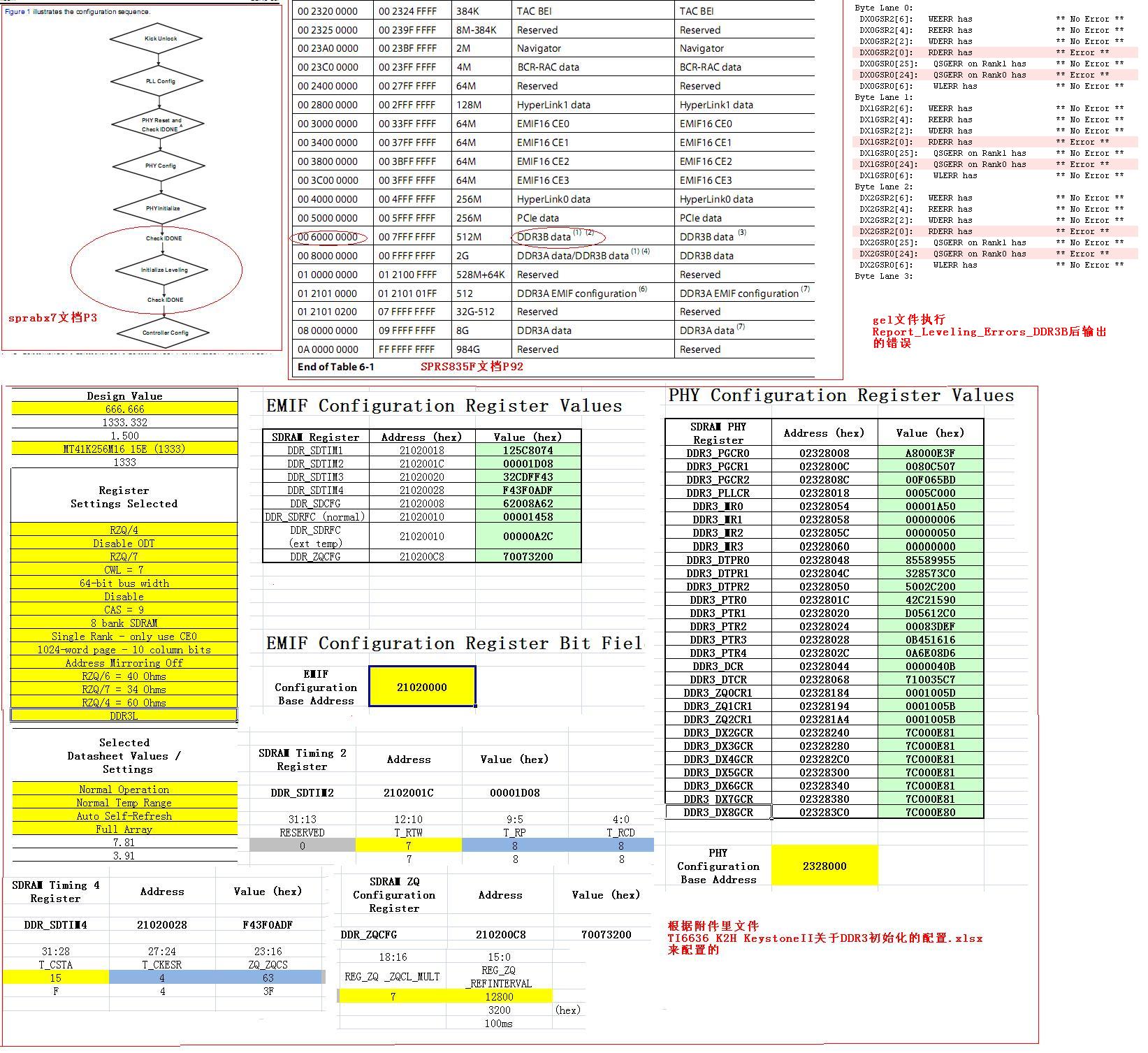
gel文件中DDR3B的执行,寄存器的基地址以及偏移都是对的。
/*----------------------------------------------------- DDR3B : debug, 64bit--------------------------------------------------------------------------*/
ddr3B_64bit_setup(int ECC_Enable)
{ //DDR3_PLL_333
unsigned int multiplier = 19;
unsigned int divider = 0;
unsigned int OD_val = 6;
int temp,i;
int delay = 2000;
KICK0 = 0x83E70B13;
KICK1 = 0x95A4F1E0;
// Poll for IDONE=1 in the PHY General Status Register 0 (address offset 0x010).
do
{
read_val = DDR3B_PGSR0;
} while ((read_val&0x00000001) != 0x00000001);
//Clocks are enabled and frequency is stable---------------------------------------
//DDR3B PLL setup
GEL_TextOut ( "DDR3B PLL Setup ... \n");
DDR3BPLLCTL0 = DDR3BPLLCTL0 & 0xFF7FFFFF;
//Set ENSAT = 1
DDR3BPLLCTL1 |= 0x00000040;
// Put the PLL in PLL Mode
DDR3BPLLCTL0 |= 0x00800000;
//Program the necessary multipliers/dividers and BW adjustments
//Set the divider values
DDR3BPLLCTL0 &= ~(0x0000003F);
DDR3BPLLCTL0 |= (divider & 0x0000003F);
//Program OD[3:0] in the SECCTL register
DDR3BPLLCTL0 &= OUTPUT_DIVIDE_MASK; // clear the OD bit field
DDR3BPLLCTL0 |= ~OUTPUT_DIVIDE_MASK & (OD_val - 1) << OUTPUT_DIVIDE_OFFSET; // set the OD[3:0] bit field of PLLD to OD_val
// Set the Multipler values
DDR3BPLLCTL0 &= ~(0x0007FFC0);
DDR3BPLLCTL0 |= ((multiplier << 6) & 0x0007FFC0 );
// Set BWADJ
temp = ((multiplier + 1) >> 1) - 1;
DDR3BPLLCTL0 &= ~(0xFF000000);
DDR3BPLLCTL0 |= ((temp << 24) & 0xFF000000);
DDR3BPLLCTL1 &= ~(0x0000000F);
DDR3BPLLCTL1 |= ((temp >> 8) & 0x0000000F);
// In PLL Controller, reset the PLL (bit 13 in DDR3BPLLCTL1 register)
DDR3BPLLCTL1 |= 0x00004000;
for(i=0;i<delay;i++);
// In DDR3PLLCTL1, write PLLRST = 0 to bring PLL out of reset
DDR3BPLLCTL1 &= ~(0x00004000);
for(i=0;i<delay;i++);
// Put the PLL in PLL Mode Switch to PLL mode
DDR3BPLLCTL0 &= ~(0x00800000); // ReSet the Bit 23
GEL_TextOut( "Lammar DDR3 PLL Setup complete, DDR3B clock now running at 666MHz.\n" );
/*------------------------------- ECO FIX -----------------------------------------*/
/*DDR3 PHY Initialization*/
// DDR3 write leveling ECO - Assert & release DDR PHY RESET after DDR PLL setup...
DDR3BPLLCTL1 = DDR3BPLLCTL1 | 0x80000000; //Assert DDR PHY reset after PLL enabled
for(i=0;i<delay;i++); //delay 1000 cycles
DDR3BPLLCTL1 = DDR3BPLLCTL1 & 0x7FFFFFFF; //Release DDR PHY reset
do
{ // Poll IDONE after resetting PHY
read_val = DDR3B_PGSR0;
} while ((read_val&0x00000001) != 0x00000001);
/*------------------------- Start PHY Configuration -------------------------------*/
// Program FRQSEL in the PLL Control Register (address offset 0x018).
DDR3B_PLLCR = 0x0005C000; //Set FRQSEL=11, for ctl_clk between 166-275MHz
// Program WLSTEP=1, IODDRM=1, and ZCKSEL in the PHY General Configuration Register 1 (address offset 0x00C).
DDR3B_PGCR1 =0x0080C507;
// Program PHY Timing Parameters Register 0-4 (address offset 0x01C - 0x02C).
DDR3B_PTR0 = 0x42C21590;
DDR3B_PTR1 = 0xD05612C0;
DDR3B_PTR2 = 0x00083DEF;
// Maintain default values of Phy Timing Parameters Register 2 in PUB
DDR3B_PTR3 = 0x0B451616;
DDR3B_PTR4 = 0x0A6E08D6;
// Program PDQ, MPRDQ, and BYTEMASK in the DRAM Configuration Register (address offset 0x044).
// All other fields must be left at their default values.
DDR3B_DCR=0x0000040B;
read_val = DDR3B_DCR;
GEL_TextOut("DDR3B_DCR = %x\n",,,,, read_val);
//Program DRAM Timing Parameters Register 0-2 (address offset 0x048 - 0x050).
DDR3B_DTPR0 = 0x85589955;//code
DDR3B_DTPR1 = 0x328573C0;
DDR3B_DTPR2 = 0x5002C200;
// Program BL=0, CL, WR, and PD=1 in the Mode Register 0 (address offset 0x054).
// All other fields must be left at their default values.
DDR3B_MR0 = 0x00001A50;
// Program DIC, RTT, and TDQS in the Mode Register 1 (address offset 0x058).
// All other fields must be left at their default values.
DDR3B_MR1 = 0x00000006;
// Program Mode Register 2 (address offset 0x05C).
DDR3B_MR2 = 0x00000050;
DDR3B_MR3 = 0x0;
// Program DTMPR=1, DTEXD, DTEXG, RANKEN=1 or 3, and RFSHDT=7 in the Data Training Configuration Register (address offset 0x068).
// All other fields must be left at their default values.
DDR3B_DTCR = 0x710035C7; //Single-rank
// Program tREFPRD=(5*tREFI/ddr_clk_period) in the PHY General Configuration Register 2 (address offset 0x08C).
//All other fields must be left at their default values.
DDR3B_PGCR2 = 0x00F065BD;
DDR3B_PGCR0 = 0xA8000E3F;
DDR3B_PGCR1 = 0x0080C507;
//Set Impedence Register and DFIPU0=1
DDR3B_ZQ0CR1 = 0x0001005D;
DDR3B_ZQ1CR1 = 0x0001005B;
DDR3B_ZQ2CR1 = 0x0001005B;
// Re-trigger PHY initialization in DDR PHY through the VBUSP interface.
// Program 0x00000033 to the PHY Initialization Register (address offset 0x004) to re-trigger PLL, ZCAL, and DCAL initialization.
DDR3B_PIR = 0x00000033;
// Poll for IDONE=1 in the PHY General Status Register 0 (address offset 0x010).
do
{
read_val = DDR3B_PGSR0;
} while ((read_val&0x00000001) != 0x00000001);
//---------------------------------------------------------------------------------------------------------
/*DDR3B_DX2GCR = 0x7C000E81;
DDR3B_DX3GCR = 0x7C000E81;
DDR3B_DX4GCR = 0x7C000E81;
DDR3B_DX5GCR = 0x7C000E81;
DDR3B_DX6GCR = 0x7C000E81;
DDR3B_DX7GCR = 0x7C000E81;
DDR3B_DX8GCR = 0x7C000E80;
*/
if(!ECC_Enable)
{
GEL_TextOut("DDR3B_DATX8_8 Front = %x\n",,,,, read_val);
read_val =DDR3B_DATX8_8 ;
DDR3B_DATX8_8 = read_val & 0xFFFFFFFE; //Disable ECC byte lane
GEL_TextOut("DDR3B_DATX8_8 rear = %x\n",,,,, DDR3B_DATX8_8);
}
// Trigger DDR3 initialization and leveling/training in DDR PHY through the VBUSP interface.
// If using a 16-bit wide DDR interface, program DXEN=0 in the DATX8 2-7 General Configuration Registers (address offsets 0x240, 0x280, 0x2C0, 0x300, 0x340, and 0x380) to disable the leveling/training for the upper byte lanes.
// If using a 32-bit wide DDR interface, program DXEN=0 in the DATX8 4-7 General Configuration Registers (address offsets 0x2C0, 0x300, 0x340, and 0x380) to disable the leveling/training for the upper byte lanes.
// If ECC is not required, program DXEN=0 in the DATX8 8 General Configuration Register (address offset 0x3C0) to disable the leveling/training for the ECC byte lane.
// NOTE: Setup supports 64-bit by default, ECC enable by default.
// Program 0x0000XF81 to the PHY Initialization Register (address offset 0x004) to trigger DDR3 initialization and leveling/training sequences
DDR3B_PIR = 0x0000FF81; //WLADJ - ON
//---------------------------------------------------------------------------------------------------------
GEL_TextOut("DDR3B_leveling starting....\r\n");
// Poll for IDONE=1 in the PHY General Status Register 0 (address offset 0x010).
do {
read_val = DDR3B_PGSR0;
} while ((read_val&0x00000001) != 0x00000001);
GEL_TextOut("DDR3B_leveling over\r\n");
/* End PHY Configuration */
if(ECC_Enable)
{
GEL_TextOut("\nECC_Enable ECC_Enable ECC_Enable");
//Enable ECC
//0xB0000000: ECC_EN=1, ECC_VERIFY_EN=1, RMW_EN=1
//0x50000000: ECC_EN=1, ECC_VERIFY_EN=0, RMW_EN=1
DDR3B_ECC_CTRL = 0xB0000000;
read_val = DDR3B_ECC_CTRL;
if(read_val!=0xB0000000){
GEL_TextOut("\nIncorrect data written to DDR3B_ECC_CTRL..");
}
}
GEL_TextOut("PHY Config Complete.... \r\n");
//---------------------------------------------------------------------------------------------------------
//For single rank, EBANK field in DDR_SDCFG register needs to be programmed to 0x0.
DDR3B_SDCFG = 0x62008A62; //Single-Rank--
DDR3B_SDTIM1 = 0x125C8074;
DDR3B_SDTIM2 = 0x00001D08;
DDR3B_SDTIM3 = 0x32CDFF43;
DDR3B_SDTIM4 = 0xF43F0ADF;
//For single rank, ZQCFG needs to be programmed to 0x70073200.
DDR3B_ZQCFG = 0x70073200; //Single-Rank 0x70073200
// Program reg_initref_dis=0 in the SDRAM Refresh Control Register (address offset 0x10).
DDR3B_SDRFC = 0x00001458;//0x00000A2C
read_val = DDR3B_PGSR0;
GEL_TextOut("DDR3B_PGSR0 = %x\n",,,,, read_val);
read_val = DDR3B_PGSR1;
GEL_TextOut("DDR3B_PGSR1 = %x\n",,,,, read_val);
GEL_TextOut("DDR3B 1600 initialization complete \n");
/* End DDR3B EMIF Configuration */
}
arm_A15_0: GEL Output: DDR3B PLL Setup ...
arm_A15_0: GEL Output: Lammar DDR3 PLL Setup complete, DDR3B clock now running at 666MHz.
arm_A15_0: GEL Output: DDR3B_DCR = 0x0000040B
arm_A15_0: GEL Output: DDR3B_DATX8_8 Front = 0xB000000F
arm_A15_0: GEL Output: DDR3B_DATX8_8 rear = 0xB000000E
arm_A15_0: GEL Output: DDR3B_PGSR0 = 0xB1C001FF
arm_A15_0: GEL Output: DDR3B_PGSR1 = 0x00000000
arm_A15_0: GEL Output: DDR3B 1333M initialization complete
arm_A15_0: GEL Output: ****************************************************************************************************************
arm_A15_0: GEL Output: ********************************************************
arm_A15_0: GEL Output: ****************************************************************************************************************
arm_A15_0: GEL Output: ***************** DDR3B Leveling Errors *********************
arm_A15_0: GEL Output: PGSR0[27]: WEERR has ** No Error **
arm_A15_0: GEL Output: PGSR0[26]: REERR has ** No Error **
arm_A15_0: GEL Output: PGSR0[25]: WDERR has ** No Error **
arm_A15_0: GEL Output: PGSR0[24]: RDERR has ** Error **
arm_A15_0: GEL Output: PGSR0[23]: WLAERR has ** Error **
arm_A15_0: GEL Output: PGSR0[22]: QSGERR has ** Error **
arm_A15_0: GEL Output: PGSR0[21]: WLERR has ** No Error **
arm_A15_0: GEL Output: PGSR0[20]: ZCERR has ** No Error **
arm_A15_0: GEL Output: PGSR0[11]: WEDONE is ** Not Set **
arm_A15_0: GEL Output: PGSR0[10]: REDONE is ** Not Set **
arm_A15_0: GEL Output: PGSR0[9]: WDDONE is ** Not Set **
arm_A15_0: GEL Output: PGSR0[8]: RDDONE is ** Set **
arm_A15_0: GEL Output: PGSR0[7]: WLADONE is ** Set **
arm_A15_0: GEL Output: PGSR0[6]: QSGDONE is ** Set **
arm_A15_0: GEL Output: PGSR0[5]: WLDONE is ** Set **
arm_A15_0: GEL Output: PGSR0[4]: DIDONE is ** Set **
arm_A15_0: GEL Output: PGSR0[3]: ZCDONE is ** Not Set **
arm_A15_0: GEL Output: PGSR0[2]: DCDONE is ** Set **
arm_A15_0: GEL Output: PGSR0[1]: PLDONE is ** Set **
arm_A15_0: GEL Output: PGSR0[0]: IDONE is ** Set **
arm_A15_0: GEL Output: ********************************************************
arm_A15_0: GEL Output: Leveling Errors by Byte Lane:
arm_A15_0: GEL Output: Byte Lane 0:
arm_A15_0: GEL Output: DX0GSR2[6]: WEERR has ** No Error **
arm_A15_0: GEL Output: DX0GSR2[4]: REERR has ** No Error **
arm_A15_0: GEL Output: DX0GSR2[2]: WDERR has ** No Error **
arm_A15_0: GEL Output: DX0GSR2[0]: RDERR has ** Error **
arm_A15_0: GEL Output: DX0GSR0[25]: QSGERR on Rank1 has ** No Error **
arm_A15_0: GEL Output: DX0GSR0[24]: QSGERR on Rank0 has ** Error **
arm_A15_0: GEL Output: DX0GSR0[6]: WLERR has ** No Error **
arm_A15_0: GEL Output: Byte Lane 1:
arm_A15_0: GEL Output: DX1GSR2[6]: WEERR has ** No Error **
arm_A15_0: GEL Output: DX1GSR2[4]: REERR has ** No Error **
arm_A15_0: GEL Output: DX1GSR2[2]: WDERR has ** No Error **
arm_A15_0: GEL Output: DX1GSR2[0]: RDERR has ** Error **
arm_A15_0: GEL Output: DX1GSR0[25]: QSGERR on Rank1 has ** No Error **
arm_A15_0: GEL Output: DX1GSR0[24]: QSGERR on Rank0 has ** Error **
arm_A15_0: GEL Output: DX1GSR0[6]: WLERR has ** No Error **
arm_A15_0: GEL Output: Byte Lane 2:
arm_A15_0: GEL Output: DX2GSR2[6]: WEERR has ** No Error **
arm_A15_0: GEL Output: DX2GSR2[4]: REERR has ** No Error **
arm_A15_0: GEL Output: DX2GSR2[2]: WDERR has ** No Error **
arm_A15_0: GEL Output: DX2GSR2[0]: RDERR has ** Error **
arm_A15_0: GEL Output: DX2GSR0[25]: QSGERR on Rank1 has ** No Error **
arm_A15_0: GEL Output: DX2GSR0[24]: QSGERR on Rank0 has ** Error **
arm_A15_0: GEL Output: DX2GSR0[6]: WLERR has ** No Error **
arm_A15_0: GEL Output: Byte Lane 3:
arm_A15_0: GEL Output: DX3GSR2[6]: WEERR has ** No Error **
arm_A15_0: GEL Output: DX3GSR2[4]: REERR has ** No Error **
arm_A15_0: GEL Output: DX3GSR2[2]: WDERR has ** No Error **
arm_A15_0: GEL Output: DX3GSR2[0]: RDERR has ** Error **
arm_A15_0: GEL Output: DX3GSR0[25]: QSGERR on Rank1 has ** No Error **
arm_A15_0: GEL Output: DX3GSR0[24]: QSGERR on Rank0 has ** Error **
arm_A15_0: GEL Output: DX3GSR0[6]: WLERR has ** No Error **
arm_A15_0: GEL Output: Byte Lane 4:
arm_A15_0: GEL Output: DX4GSR2[6]: WEERR has ** No Error **
arm_A15_0: GEL Output: DX4GSR2[4]: REERR has ** No Error **
arm_A15_0: GEL Output: DX4GSR2[2]: WDERR has ** No Error **
arm_A15_0: GEL Output: DX4GSR2[0]: RDERR has ** Error **
arm_A15_0: GEL Output: DX4GSR0[25]: QSGERR on Rank1 has ** No Error **
arm_A15_0: GEL Output: DX4GSR0[24]: QSGERR on Rank0 has ** Error **
arm_A15_0: GEL Output: DX4GSR0[6]: WLERR has ** No Error **
arm_A15_0: GEL Output: Byte Lane 5:
arm_A15_0: GEL Output: DX5GSR2[6]: WEERR has ** No Error **
arm_A15_0: GEL Output: DX5GSR2[4]: REERR has ** No Error **
arm_A15_0: GEL Output: DX5GSR2[2]: WDERR has ** No Error **
arm_A15_0: GEL Output: DX5GSR2[0]: RDERR has ** Error **
arm_A15_0: GEL Output: DX5GSR0[25]: QSGERR on Rank1 has ** No Error **
arm_A15_0: GEL Output: DX5GSR0[24]: QSGERR on Rank0 has ** Error **
arm_A15_0: GEL Output: DX5GSR0[6]: WLERR has ** No Error **
arm_A15_0: GEL Output: Byte Lane 6:
arm_A15_0: GEL Output: DX6GSR2[6]: WEERR has ** No Error **
arm_A15_0: GEL Output: DX6GSR2[4]: REERR has ** No Error **
arm_A15_0: GEL Output: DX6GSR2[2]: WDERR has ** No Error **
arm_A15_0: GEL Output: DX6GSR2[0]: RDERR has ** Error **
arm_A15_0: GEL Output: DX6GSR0[25]: QSGERR on Rank1 has ** No Error **
arm_A15_0: GEL Output: DX6GSR0[24]: QSGERR on Rank0 has ** Error **
arm_A15_0: GEL Output: DX6GSR0[6]: WLERR has ** No Error **
arm_A15_0: GEL Output: Byte Lane 7:
arm_A15_0: GEL Output: DX7GSR2[6]: WEERR has ** No Error **
arm_A15_0: GEL Output: DX7GSR2[4]: REERR has ** No Error **
arm_A15_0: GEL Output: DX7GSR2[2]: WDERR has ** No Error **
arm_A15_0: GEL Output: DX7GSR2[0]: RDERR has ** Error **
arm_A15_0: GEL Output: DX7GSR0[25]: QSGERR on Rank1 has ** No Error **
arm_A15_0: GEL Output: DX7GSR0[24]: QSGERR on Rank0 has ** Error **
arm_A15_0: GEL Output: DX7GSR0[6]: WLERR has ** No Error **
arm_A15_0: GEL Output: Byte Lane 8:
arm_A15_0: GEL Output: DX8GSR2[6]: WEERR has ** No Error **
arm_A15_0: GEL Output: DX8GSR2[4]: REERR has ** No Error **
arm_A15_0: GEL Output: DX8GSR2[2]: WDERR has ** No Error **
arm_A15_0: GEL Output: DX8GSR2[0]: RDERR has ** No Error **
arm_A15_0: GEL Output: DX8GSR0[25]: QSGERR on Rank1 has ** No Error **
arm_A15_0: GEL Output: DX8GSR0[24]: QSGERR on Rank0 has ** No Error **
arm_A15_0: GEL Output: DX8GSR0[6]: WLERR has ** No Error **
arm_A15_0: GEL Output: ****************************************************************************************************************
0880.TI6636 K2H KeystoneII关于DDR3初始化的配置.xlsx
3060.Silicon Errata(sprz399d).pdf
arm_A15_0: GEL Output: DDR3B PLL Setup ...
arm_A15_0: GEL Output: Lammar DDR3 PLL Setup complete, DDR3B clock now running at 666MHz.
arm_A15_0: GEL Output: DDR3B_DCR = 0x0000040B
arm_A15_0: GEL Output: DDR3B_DATX8_8 Front = 0xB000000F
arm_A15_0: GEL Output: DDR3B_DATX8_8 rear = 0xB000000E
arm_A15_0: GEL Output: DDR3B_PGSR0 = 0xB1C001FF
arm_A15_0: GEL Output: DDR3B_PGSR1 = 0x00000000
arm_A15_0: GEL Output: DDR3B 1600 initialization complete
arm_A15_0: GEL Output: ****************************************************************************************************************
arm_A15_0: GEL Output: ********************************************************
arm_A15_0: GEL Output: DDR PLL Registers:

arm_A15_0: GEL Output:  DDR3B_PLL_CTL0 register:  0x092804C0 (0x02620368)
arm_A15_0: GEL Output:  	PLLD[5:0]:		0 (Pre-Divide value of 1)
arm_A15_0: GEL Output:  	PLLM[18:6]:		19 (Multiplier value of 20)
arm_A15_0: GEL Output:  	CLKOD[22:19]:		5 (Output Divide value of 6)
arm_A15_0: GEL Output:  	BYPASS[23]:		0
arm_A15_0: GEL Output:  	BWADJ-lower[31:24]: 	9
arm_A15_0: GEL Output:  DDR3B_PLL_CTL1 register:  0x00000040
arm_A15_0: GEL Output:  	PLLRESET[14]: Reset ** DEASSERTED ** to PLL
arm_A15_0: GEL Output:  	ENSAT[6]: ENSAT is SET - (GOOD)
arm_A15_0: GEL Output:  	BWADJ-upper[3:0]:	0
arm_A15_0: GEL Output:  	BWADJ[11:0] (combined):	9
arm_A15_0: GEL Output: ****************************************************************************************************************
arm_A15_0: GEL Output: ****************************************************************************************************************
arm_A15_0: GEL Output: ********************************************************
arm_A15_0: GEL Output: DDR SDRAM Configuration Register (SDCFG)
arm_A15_0: GEL Output: DDR3BEMIF_SDCFG:			0x6200CE62 (Address: 0x21020008)
arm_A15_0: GEL Output: 	SDRAM Type[31:29]:   		DDR3 (3)
arm_A15_0: GEL Output: 	SDRAM Drive[27:25]:  		RZQ/4 (1)
arm_A15_0: GEL Output: 	Dynamic ODT[23:22]:  		OFF (0)
arm_A15_0: GEL Output: 	CAS Write Latency[16:14]:	8 (3)
arm_A15_0: GEL Output: 	Data Bus Width[13:12]: 		64-bit (0)
arm_A15_0: GEL Output: 	CAS Latency[11:8]:		11 (14)
arm_A15_0: GEL Output: 	Banks per SDRAM[6:5]: 		8 (3)
arm_A15_0: GEL Output: 	Chip Select Setup[3]: 		DCE0# (0)
arm_A15_0: GEL Output: 	Page Size[1:0]:    		1024 word page (2)
arm_A15_0: GEL Output: ********************************************************

arm_A15_0: GEL Output: ********************************************************
arm_A15_0: GEL Output: SDRAM Refresh Control Register (SDRFC)
arm_A15_0: GEL Output: DDR3BEMIF_SDRFC:			0x00001869 (Address: 0x21020010)
arm_A15_0: GEL Output: 	INITREF_DIS[31]:		Normal operation
arm_A15_0: GEL Output: 	REFRESH_RATE[15:0]:		6249 (REFRESH_RATE = Refresh period * DDR3 clock frequency.)
arm_A15_0: GEL Output: ********************************************************

arm_A15_0: GEL Output: ********************************************************
arm_A15_0: GEL Output: SDRAM Timing 1 Register (SDTIM1)
arm_A15_0: GEL Output: DDR3BEMIF_SDTIM1:			0x166C9855 (Address: 0x21020018)
arm_A15_0: GEL Output: 	T_WR[29:25]:			11 cycles (+1)
arm_A15_0: GEL Output: 	T_RAS[24:18]:			27 cycles (+1)
arm_A15_0: GEL Output: 	T_RC[17:10]:			38 cycles (+1)
arm_A15_0: GEL Output: 	T_RRD[9:4]:			5 cycles (+1)
arm_A15_0: GEL Output: 	T_WTR[3:0]:			5 cycles (+1)
arm_A15_0: GEL Output: ********************************************************

arm_A15_0: GEL Output: ********************************************************
arm_A15_0: GEL Output: SDRAM Timing 2 Register (SDTIM2)
arm_A15_0: GEL Output: DDR3BEMIF_SDTIM2:			0x00001D4A (Address: 0x2102001C)
arm_A15_0: GEL Output: 	T_RTW[12:10]:			7 cycles (+1)
arm_A15_0: GEL Output: 	T_RP[9:5]:			10 cycles (+1)
arm_A15_0: GEL Output: 	T_RCD[4:0]:			10 cycles (+1)
arm_A15_0: GEL Output: ********************************************************

arm_A15_0: GEL Output: ********************************************************
arm_A15_0: GEL Output: SDRAM Timing 3 Register (SDTIM3)
arm_A15_0: GEL Output: DDR3BEMIF_SDTIM3:			0x35DFF53A (Address: 0x21020020)
arm_A15_0: GEL Output: 	T_XP[31:28]:			3 cycles (+1)
arm_A15_0: GEL Output: 	T_XSNR[27:18]:			375 cycles (+1)
arm_A15_0: GEL Output: 	T_XSRD[17:8]:			1013 cycles (+1)
arm_A15_0: GEL Output: 	T_RTP[7:4]:			3 cycles (+1)
arm_A15_0: GEL Output: 	T_CKE[3:0]:			10 cycles (+1)
arm_A15_0: GEL Output: ********************************************************

arm_A15_0: GEL Output: ********************************************************
arm_A15_0: GEL Output: SDRAM Timing 4 Register (SDTIM4)
arm_A15_0: GEL Output: 	DDR3BEMIF_SDTIM4:		0x543F0CFF (Address: 0x21020028)
arm_A15_0: GEL Output: 	T_CSTA[31:28]:			3 cycles (+1)
arm_A15_0: GEL Output: 	T_CKESR[27:24]:			5 cycles (+1)
arm_A15_0: GEL Output: 	ZQ_ZQCS[23:16]:			223 cycles (+1)
arm_A15_0: GEL Output: 	T_RFC[13:4]:			851 cycles (+1)
arm_A15_0: GEL Output: 	T_RAS_MAX[3:0]:(should be 0xF)	10 cycles
arm_A15_0: GEL Output: ********************************************************

arm_A15_0: GEL Output: ********************************************************
arm_A15_0: GEL Output: SDRAM Output Impedance Calibration Configuration Register (ZQCFG)
arm_A15_0: GEL Output: 	DDR3BEMIF_ZQCFG:		0x70073200 (Address: 0x210200C8)
arm_A15_0: GEL Output: 	ZQ_CS1EN[31]:			ZQ calibration for Rank 2 is Disabled (0)
arm_A15_0: GEL Output: 	ZQ_CS0EN[31]:			ZQ calibration for Rank 1 is Enabled (1)
arm_A15_0: GEL Output: 	ZQ_DUALCALEN[29]:		Dual ZQ calibration is Enabled (1)
arm_A15_0: GEL Output: 	ZQ_SFEXITEN[28]:		ZQ calibration on self-refresh, Active power-down and precharge power-down exit is Enabled (1)
arm_A15_0: GEL Output: 	ZQ_ZQCL_MULT[18:16]:		7 cycles
arm_A15_0: GEL Output: 	ZQ_REFINTERVAL[15:0]:		Refresh periods between ZQCS commands is 12800 (+1)
arm_A15_0: GEL Output: ********************************************************
arm_A15_0: GEL Output: ****************************************************************************************************************

arm_A15_0: GEL Output: ********************************************************
arm_A15_0: GEL Output: PLL Control Register (PLLCR)
arm_A15_0: GEL Output: DDR3B_PLLCR:			0x000DE000 (Address: 0x02328018)
arm_A15_0: GEL Output: 	FRQSEL[19:18]:			PLL Reference clock ranges from 166MHz to 275MHz (3)
arm_A15_0: GEL Output: Note: PLL Reference Clock should be 1/4 of DDR data rate. (i.e. 400MHz -> 1600MTs)
arm_A15_0: GEL Output: ********************************************************

arm_A15_0: GEL Output: ********************************************************
arm_A15_0: GEL Output: DRAM Timing Parameters Register 0 (DTPR0)
arm_A15_0: GEL Output: DDR3B_DTPR0:			0x8558AA75 (Address: 0x02328048)
arm_A15_0: GEL Output: 	tRFC[31:26]:			Activate to Activate command delay (same bank) is 33 cycles
arm_A15_0: GEL Output: 	tRRD[25:22]:			Activate to Activate command delay (diff banks) is 5 cycles
arm_A15_0: GEL Output: 	tRAS[21:16]:			Activate to Precharge command delay is 24 cycles
arm_A15_0: GEL Output: 	tRCD[15:12]:			Activate to Read/Write (on activated row) command delay is 10 cycles
arm_A15_0: GEL Output: 	tRP[11:8]:			Precharge command period is 10 cycles
arm_A15_0: GEL Output: 	tWTR[7:4]:			Internal write to read command delay is 7 cycles
arm_A15_0: GEL Output: 	tRTP[3:0]:			Internal read to precharge command delay is 5 cycles
arm_A15_0: GEL Output: ********************************************************

arm_A15_0: GEL Output: ********************************************************
arm_A15_0: GEL Output: DRAM Timing Parameters Register 1 (DTPR1)
arm_A15_0: GEL Output: DDR3B_DTPR1:			0x32857370 (Address: 0x0232804C)
arm_A15_0: GEL Output: 	tWLO[29:26]:			Write leveling output delay is 12 cycles
arm_A15_0: GEL Output: 	tWLMRD[25:20]:			Min delay from write leveling mode to first DQS edge is 40 cycles
arm_A15_0: GEL Output: 	tRFC[19:11]:			Refresh to Refresh command delay is 174 cycles
arm_A15_0: GEL Output: 	tFAW[10:5]:			4-bank activate period is 27 cycles
arm_A15_0: GEL Output: 	tMOD[4:2]:			Load mode update delay is Reserved Value cycles (16)
arm_A15_0: GEL Output: 	tMRD[1:0]:			Load mode cycle time is 0 cycles
arm_A15_0: GEL Output: ********************************************************

arm_A15_0: GEL Output: ********************************************************
arm_A15_0: GEL Output: DRAM Timing Parameters Register 2 (DTPR2)
arm_A15_0: GEL Output: DDR3B_DTPR2:			0x5002C200 (Address: 0x02328050)
arm_A15_0: GEL Output: 	tCCD[31]:			Read to read and write to write command delay is 4 cycles (0)
arm_A15_0: GEL Output: 	tRTW[30]:			Read to write command delay is standard bus turn around delay +1 clock (1)
arm_A15_0: GEL Output: 	tRTODT[29]:			Read to ODT delay is 0, may come immediately after read post-amble (0)
arm_A15_0: GEL Output: 	tDLLK[28:19]:			DLL locking time is 512 cycles
arm_A15_0: GEL Output: 	tCKE[28:19]:			CKE minimum pulse width (tCKESR) is 5 cycles
arm_A15_0: GEL Output: 	tXP[14:10]:			Power down exit delay is 16 cycles
arm_A15_0: GEL Output: 	tXS[9:0]:			Self refresh exit delay is 512 cycles
arm_A15_0: GEL Output: ********************************************************
arm_A15_0: GEL Output: Mode Register 0 (MR0)
arm_A15_0: GEL Output: DDR3B_MR0:				0x00001C70 (Address: 0x02328054)
arm_A15_0: GEL Output: 	PD[12]:				Fast power down exit (DLL on) (1)
arm_A15_0: GEL Output: 	WR[11:9]:Write Recovery is 14 cycles (6)
arm_A15_0: GEL Output: 	CL[6:4,2]:			11 cycles (14)
arm_A15_0: GEL Output: ********************************************************

arm_A15_0: GEL Output: ********************************************************
arm_A15_0: GEL Output: Mode Register 1 (MR1)
arm_A15_0: GEL Output: DDR3B_MR1:				0x00000006 (Address: 0x02328058)
arm_A15_0: GEL Output: 	AL[4:3]:			AL Disabled (0)
arm_A15_0: GEL Output: 	RTT[9,6,2]:			ODT is RZQ/4 on SDRAM (1)
arm_A15_0: GEL Output: 	DIC[5,1]:			Output Drive is RZQ/7 on SDRAM (1)
arm_A15_0: GEL Output: 	DE[0]:				DLL Enabled on SDRAM (0)
arm_A15_0: GEL Output: ********************************************************

arm_A15_0: GEL Output: ********************************************************
arm_A15_0: GEL Output: Mode Register 2 (MR2)
arm_A15_0: GEL Output: DDR3B_MR2:				0x00000018 (Address: 0x0232805C)
arm_A15_0: GEL Output: 	RTTWR[10:9]:			Dynamic ODT is Disabled (0)
arm_A15_0: GEL Output: 	CWL[5:3]:			CAS Write Latency is 8 cycles (3)
arm_A15_0: GEL Output: 	SRT[7]:				Normal Operating Temperature Range (0)
arm_A15_0: GEL Output: 	ASR[6]:				Auto Self-Refresh Power Management Disabled (0)
arm_A15_0: GEL Output: 	PASR[2:0]:			Partial Array Self-Refresh is set to Full Array (0)
arm_A15_0: GEL Output: ********************************************************

arm_A15_0: GEL Output: ********************************************************
arm_A15_0: GEL Output: Impedance Control Register 1 (ACC signals) (ZQ0CR1)
arm_A15_0: GEL Output: DDR3B_ZQ0CR1:			0x0001005D (Address: 0x02328184)
arm_A15_0: GEL Output: 	ZPROG-ODT[7:4]:			On-Die Termination is set to N/A (5)
arm_A15_0: GEL Output: 	ZPROG-ZO[3:0]:			Output Impedance is set to 34ohms (13)
arm_A15_0: GEL Output: ********************************************************

arm_A15_0: GEL Output: ********************************************************
arm_A15_0: GEL Output: Impedance Control Register 1 (Data Lanes 0-3) (ZQ1CR1)
arm_A15_0: GEL Output: DDR3B_ZQ1CR1:			0x0001005B (Address: 0x02328194)
arm_A15_0: GEL Output: 	ZPROG-ODT[7:4]:			On-Die Termination is set to 60ohms (5)
arm_A15_0: GEL Output: 	ZPROG-ZO[3:0]:			Output Impedance is set to 40ohms (11)
arm_A15_0: GEL Output: ********************************************************

arm_A15_0: GEL Output: ********************************************************
arm_A15_0: GEL Output: Impedance Control Register 1 (Data Lanes 4-7) (ZQ2CR1)
arm_A15_0: GEL Output: DDR3B_ZQ2CR1:			0x0001005B (Address: 0x023281A4)
arm_A15_0: GEL Output: 	ZPROG-ODT[7:4]:			On-Die Termination is set to 60ohms (5)
arm_A15_0: GEL Output: 	ZPROG-ZO[3:0]:			Output Impedance is set to 40ohms (11)
arm_A15_0: GEL Output: ********************************************************

arm_A15_0: GEL Output: ****************************************************************************************************************
arm_A15_0: GEL Output: ***************** DDR3B Leveling Errors *********************
arm_A15_0: GEL Output:  PGSR0[27]:	WEERR has 	** No Error **
arm_A15_0: GEL Output:  PGSR0[26]:	REERR has 	** No Error **
arm_A15_0: GEL Output:  PGSR0[25]:	WDERR has 	** No Error **
arm_A15_0: GEL Output:  PGSR0[24]:	RDERR has 	** Error **
arm_A15_0: GEL Output:  PGSR0[23]:	WLAERR has 	** Error **
arm_A15_0: GEL Output:  PGSR0[22]:	QSGERR has 	** Error **
arm_A15_0: GEL Output:  PGSR0[21]:	WLERR has 	** No Error **
arm_A15_0: GEL Output:  PGSR0[20]:	ZCERR has 	** No Error **

arm_A15_0: GEL Output:  PGSR0[11]:	WEDONE is 	** Not Set **
arm_A15_0: GEL Output:  PGSR0[10]:	REDONE is 	** Not Set **
arm_A15_0: GEL Output:  PGSR0[9]:		WDDONE is 	** Not Set **
arm_A15_0: GEL Output:  PGSR0[8]:		RDDONE is 	** Set **
arm_A15_0: GEL Output:  PGSR0[7]:		WLADONE is 	** Set **
arm_A15_0: GEL Output:  PGSR0[6]:		QSGDONE is 	** Set **
arm_A15_0: GEL Output:  PGSR0[5]:		WLDONE is 	** Set **
arm_A15_0: GEL Output:  PGSR0[4]:		DIDONE is 	** Set **
arm_A15_0: GEL Output:  PGSR0[3]:		ZCDONE is 	** Not Set **
arm_A15_0: GEL Output:  PGSR0[2]:		DCDONE is 	** Set **
arm_A15_0: GEL Output:  PGSR0[1]:		PLDONE is 	** Set **
arm_A15_0: GEL Output:  PGSR0[0]:		IDONE is 	** Set **

arm_A15_0: GEL Output: ********************************************************
arm_A15_0: GEL Output: Leveling Errors by Byte Lane:

arm_A15_0: GEL Output: Byte Lane 0:
arm_A15_0: GEL Output: 	DX0GSR2[6]:   WEERR has 		** No Error **
arm_A15_0: GEL Output: 	DX0GSR2[4]:   REERR has 		** No Error **
arm_A15_0: GEL Output: 	DX0GSR2[2]:   WDERR has 		** No Error **
arm_A15_0: GEL Output: 	DX0GSR2[0]:   RDERR has 		** Error **
arm_A15_0: GEL Output: 	DX0GSR0[25]:   QSGERR on Rank1 has 	** No Error **
arm_A15_0: GEL Output: 	DX0GSR0[24]:   QSGERR on Rank0 has 	** Error **
arm_A15_0: GEL Output: 	DX0GSR0[6]:    WLERR has 		** No Error **
arm_A15_0: GEL Output: Byte Lane 1:
arm_A15_0: GEL Output: 	DX1GSR2[6]:   WEERR has 		** No Error **
arm_A15_0: GEL Output: 	DX1GSR2[4]:   REERR has 		** No Error **
arm_A15_0: GEL Output: 	DX1GSR2[2]:   WDERR has 		** No Error **
arm_A15_0: GEL Output: 	DX1GSR2[0]:   RDERR has 		** Error **
arm_A15_0: GEL Output: 	DX1GSR0[25]:   QSGERR on Rank1 has 	** No Error **
arm_A15_0: GEL Output: 	DX1GSR0[24]:   QSGERR on Rank0 has 	** Error **
arm_A15_0: GEL Output: 	DX1GSR0[6]:    WLERR has 		** No Error **
arm_A15_0: GEL Output: Byte Lane 2:
arm_A15_0: GEL Output: 	DX2GSR2[6]:   WEERR has 		** No Error **
arm_A15_0: GEL Output: 	DX2GSR2[4]:   REERR has 		** No Error **
arm_A15_0: GEL Output: 	DX2GSR2[2]:   WDERR has 		** No Error **
arm_A15_0: GEL Output: 	DX2GSR2[0]:   RDERR has 		** Error **
arm_A15_0: GEL Output: 	DX2GSR0[25]:   QSGERR on Rank1 has 	** No Error **
arm_A15_0: GEL Output: 	DX2GSR0[24]:   QSGERR on Rank0 has 	** Error **
arm_A15_0: GEL Output: 	DX2GSR0[6]:    WLERR has 		** No Error **
arm_A15_0: GEL Output: Byte Lane 3:
arm_A15_0: GEL Output: 	DX3GSR2[6]:   WEERR has 		** No Error **
arm_A15_0: GEL Output: 	DX3GSR2[4]:   REERR has 		** No Error **
arm_A15_0: GEL Output: 	DX3GSR2[2]:   WDERR has 		** No Error **
arm_A15_0: GEL Output: 	DX3GSR2[0]:   RDERR has 		** Error **
arm_A15_0: GEL Output: 	DX3GSR0[25]:   QSGERR on Rank1 has 	** No Error **
arm_A15_0: GEL Output: 	DX3GSR0[24]:   QSGERR on Rank0 has 	** Error **
arm_A15_0: GEL Output: 	DX3GSR0[6]:    WLERR has 		** No Error **
arm_A15_0: GEL Output: Byte Lane 4:
arm_A15_0: GEL Output: 	DX4GSR2[6]:   WEERR has 		** No Error **
arm_A15_0: GEL Output: 	DX4GSR2[4]:   REERR has 		** No Error **
arm_A15_0: GEL Output: 	DX4GSR2[2]:   WDERR has 		** No Error **
arm_A15_0: GEL Output: 	DX4GSR2[0]:   RDERR has 		** Error **
arm_A15_0: GEL Output: 	DX4GSR0[25]:   QSGERR on Rank1 has 	** No Error **
arm_A15_0: GEL Output: 	DX4GSR0[24]:   QSGERR on Rank0 has 	** Error **
arm_A15_0: GEL Output: 	DX4GSR0[6]:    WLERR has 		** No Error **
arm_A15_0: GEL Output: Byte Lane 5:
arm_A15_0: GEL Output: 	DX5GSR2[6]:   WEERR has 		** No Error **
arm_A15_0: GEL Output: 	DX5GSR2[4]:   REERR has 		** No Error **
arm_A15_0: GEL Output: 	DX5GSR2[2]:   WDERR has 		** No Error **
arm_A15_0: GEL Output: 	DX5GSR2[0]:   RDERR has 		** Error **
arm_A15_0: GEL Output: 	DX5GSR0[25]:   QSGERR on Rank1 has 	** No Error **
arm_A15_0: GEL Output: 	DX5GSR0[24]:   QSGERR on Rank0 has 	** Error **
arm_A15_0: GEL Output: 	DX5GSR0[6]:    WLERR has 		** No Error **
arm_A15_0: GEL Output: Byte Lane 6:
arm_A15_0: GEL Output: 	DX6GSR2[6]:   WEERR has 		** No Error **
arm_A15_0: GEL Output: 	DX6GSR2[4]:   REERR has 		** No Error **
arm_A15_0: GEL Output: 	DX6GSR2[2]:   WDERR has 		** No Error **
arm_A15_0: GEL Output: 	DX6GSR2[0]:   RDERR has 		** Error **
arm_A15_0: GEL Output: 	DX6GSR0[25]:   QSGERR on Rank1 has 	** No Error **
arm_A15_0: GEL Output: 	DX6GSR0[24]:   QSGERR on Rank0 has 	** Error **
arm_A15_0: GEL Output: 	DX6GSR0[6]:    WLERR has 		** No Error **
arm_A15_0: GEL Output: Byte Lane 7:
arm_A15_0: GEL Output: 	DX7GSR2[6]:   WEERR has 		** No Error **
arm_A15_0: GEL Output: 	DX7GSR2[4]:   REERR has 		** No Error **
arm_A15_0: GEL Output: 	DX7GSR2[2]:   WDERR has 		** No Error **
arm_A15_0: GEL Output: 	DX7GSR2[0]:   RDERR has 		** Error **
arm_A15_0: GEL Output: 	DX7GSR0[25]:   QSGERR on Rank1 has 	** No Error **
arm_A15_0: GEL Output: 	DX7GSR0[24]:   QSGERR on Rank0 has 	** Error **
arm_A15_0: GEL Output: 	DX7GSR0[6]:    WLERR has 		** No Error **
arm_A15_0: GEL Output: Byte Lane 8:
arm_A15_0: GEL Output: 	DX8GSR2[6]:   WEERR has 		** No Error **
arm_A15_0: GEL Output: 	DX8GSR2[4]:   REERR has 		** No Error **
arm_A15_0: GEL Output: 	DX8GSR2[2]:   WDERR has 		** No Error **
arm_A15_0: GEL Output: 	DX8GSR2[0]:   RDERR has 		** No Error **
arm_A15_0: GEL Output: 	DX8GSR0[25]:   QSGERR on Rank1 has 	** No Error **
arm_A15_0: GEL Output: 	DX8GSR0[24]:   QSGERR on Rank0 has 	** No Error **
arm_A15_0: GEL Output: 	DX8GSR0[6]:    WLERR has 		** No Error **
arm_A15_0: GEL Output: ****************************************************************************************************************
arm_A15_0: GEL Output: ****************************************************************************************************************
arm_A15_0: GEL Output: ***************** DDR3B Leveling Values *********************
arm_A15_0: GEL Output: Clock Period as measured by Leveling Registers:

arm_A15_0: GEL Output:  DX0GSR0:		0x0145A320
arm_A15_0: GEL Output:  		[14:7] (Write Leveling Period): 	6
arm_A15_0: GEL Output:  		[23:16] (Read DQS Gating Period): 	69
arm_A15_0: GEL Output:  DX1GSR0:		0x0145A2A0
arm_A15_0: GEL Output:  		[14:7] (Write Leveling Period): 	5
arm_A15_0: GEL Output:  		[23:16] (Read DQS Gating Period): 	69
arm_A15_0: GEL Output:  DX2GSR0:		0x0145A2A0
arm_A15_0: GEL Output:  		[14:7] (Write Leveling Period): 	5
arm_A15_0: GEL Output:  		[23:16] (Read DQS Gating Period): 	69
arm_A15_0: GEL Output:  DX3GSR0:		0x0145A2A0
arm_A15_0: GEL Output:  		[14:7] (Write Leveling Period): 	5
arm_A15_0: GEL Output:  		[23:16] (Read DQS Gating Period): 	69
arm_A15_0: GEL Output:  DX4GSR0:		0x0145A320
arm_A15_0: GEL Output:  		[14:7] (Write Leveling Period): 	6
arm_A15_0: GEL Output:  		[23:16] (Read DQS Gating Period): 	69
arm_A15_0: GEL Output:  DX5GSR0:		0x0144A220
arm_A15_0: GEL Output:  		[14:7] (Write Leveling Period): 	4
arm_A15_0: GEL Output:  		[23:16] (Read DQS Gating Period): 	68
arm_A15_0: GEL Output:  DX6GSR0:		0x0145A320
arm_A15_0: GEL Output:  		[14:7] (Write Leveling Period): 	6
arm_A15_0: GEL Output:  		[23:16] (Read DQS Gating Period): 	69
arm_A15_0: GEL Output:  DX7GSR0:		0x0145A2A0
arm_A15_0: GEL Output:  		[14:7] (Write Leveling Period): 	5
arm_A15_0: GEL Output:  		[23:16] (Read DQS Gating Period): 	69
arm_A15_0: GEL Output:  DX8GSR0(ECC):	0x0045A380
arm_A15_0: GEL Output:  		[14:7] (Write Leveling Period): 	7
arm_A15_0: GEL Output:  		[23:16] (Read DQS Gating Period): 	69

arm_A15_0: GEL Output: ********************************************************
arm_A15_0: GEL Output: Delay Values from DDR3B Write Leveling Registers:

arm_A15_0: GEL Output:  DX0GTR:			0x00007006
arm_A15_0: GEL Output:  		[13:12] (Rank 0 WL Cycle Latency): 	3
arm_A15_0: GEL Output:  		[15:14] (Rank 1 WL Cycle Latency): 	1
arm_A15_0: GEL Output:  DX0LCDLR0:		0x00000024
arm_A15_0: GEL Output:  		[7:0] (Rank 0 WL Delay): 		36
arm_A15_0: GEL Output:  		[15:8] (Rank 1 WL Delay): 		0
arm_A15_0: GEL Output:  DX1GTR:			0x00007006
arm_A15_0: GEL Output:  		[13:12] (Rank 0 WL Cycle Latency): 	3
arm_A15_0: GEL Output:  		[15:14] (Rank 1 WL Cycle Latency): 	1
arm_A15_0: GEL Output:  DX1LCDLR0:		0x00000021
arm_A15_0: GEL Output:  		[7:0] (Rank 0 WL Delay): 		33
arm_A15_0: GEL Output:  		[15:8] (Rank 1 WL Delay): 		0
arm_A15_0: GEL Output:  DX2GTR:			0x00007006
arm_A15_0: GEL Output:  		[13:12] (Rank 0 WL Cycle Latency): 	3
arm_A15_0: GEL Output:  		[15:14] (Rank 1 WL Cycle Latency): 	1
arm_A15_0: GEL Output:  DX2LCDLR0:		0x00000020
arm_A15_0: GEL Output:  		[7:0] (Rank 0 WL Delay): 		32
arm_A15_0: GEL Output:  		[15:8] (Rank 1 WL Delay): 		0
arm_A15_0: GEL Output:  DX3GTR:			0x00005006
arm_A15_0: GEL Output:  		[13:12] (Rank 0 WL Cycle Latency): 	1
arm_A15_0: GEL Output:  		[15:14] (Rank 1 WL Cycle Latency): 	1
arm_A15_0: GEL Output:  DX3LCDLR0:		0x0000001A
arm_A15_0: GEL Output:  		[7:0] (Rank 0 WL Delay): 		26
arm_A15_0: GEL Output:  		[15:8] (Rank 1 WL Delay): 		0
arm_A15_0: GEL Output:  DX4GTR:			0x00007006
arm_A15_0: GEL Output:  		[13:12] (Rank 0 WL Cycle Latency): 	3
arm_A15_0: GEL Output:  		[15:14] (Rank 1 WL Cycle Latency): 	1
arm_A15_0: GEL Output:  DX4LCDLR0:		0x00000031
arm_A15_0: GEL Output:  		[7:0] (Rank 0 WL Delay): 		49
arm_A15_0: GEL Output:  		[15:8] (Rank 1 WL Delay): 		0
arm_A15_0: GEL Output:  DX5GTR:			0x00007006
arm_A15_0: GEL Output:  		[13:12] (Rank 0 WL Cycle Latency): 	3
arm_A15_0: GEL Output:  		[15:14] (Rank 1 WL Cycle Latency): 	1
arm_A15_0: GEL Output:  DX5LCDLR0:		0x0000002E
arm_A15_0: GEL Output:  		[7:0] (Rank 0 WL Delay): 		46
arm_A15_0: GEL Output:  		[15:8] (Rank 1 WL Delay): 		0
arm_A15_0: GEL Output:  DX6GTR:			0x00007006
arm_A15_0: GEL Output:  		[13:12] (Rank 0 WL Cycle Latency): 	3
arm_A15_0: GEL Output:  		[15:14] (Rank 1 WL Cycle Latency): 	1
arm_A15_0: GEL Output:  DX6LCDLR0:		0x00000033
arm_A15_0: GEL Output:  		[7:0] (Rank 0 WL Delay): 		51
arm_A15_0: GEL Output:  		[15:8] (Rank 1 WL Delay): 		0
arm_A15_0: GEL Output:  DX7GTR:			0x00007006
arm_A15_0: GEL Output:  		[13:12] (Rank 0 WL Cycle Latency): 	3
arm_A15_0: GEL Output:  		[15:14] (Rank 1 WL Cycle Latency): 	1
arm_A15_0: GEL Output:  DX7LCDLR0:		0x00000031
arm_A15_0: GEL Output:  		[7:0] (Rank 0 WL Delay): 		49
arm_A15_0: GEL Output:  		[15:8] (Rank 1 WL Delay): 		0
arm_A15_0: GEL Output:  DX8GTR:			0x00005000
arm_A15_0: GEL Output:  		[13:12] (Rank 0 WL Cycle Latency): 	1
arm_A15_0: GEL Output:  		[15:14] (Rank 1 WL Cycle Latency): 	1
arm_A15_0: GEL Output:  DX8LCDLR0:		0x00000000
arm_A15_0: GEL Output:  		[7:0] (Rank 0 WL Delay): 		0
arm_A15_0: GEL Output:  		[15:8] (Rank 1 WL Delay): 		0
arm_A15_0: GEL Output: ********************************************************
arm_A15_0: GEL Output: Equivalent 90 degree phase shift in delay units, derived from measured period:

arm_A15_0: GEL Output:  DX0LCDLR1:		0x00232322
arm_A15_0: GEL Output:  		[7:0] (Write Delay Shift): 		34
arm_A15_0: GEL Output:  		[15:8] (Read DQS Delay):		35
arm_A15_0: GEL Output:  		[23:16] (Read DQSN Delay): 		35
arm_A15_0: GEL Output:  DX1LCDLR1:		0x00222222
arm_A15_0: GEL Output:  		[7:0] (Write Delay Shift): 		34
arm_A15_0: GEL Output:  		[15:8] (Read DQS Delay): 		34
arm_A15_0: GEL Output:  		[23:16] (Read DQSN Delay): 		34
arm_A15_0: GEL Output:  DX2LCDLR1:		0x00232222
arm_A15_0: GEL Output:  		[7:0] (Write Delay Shift): 		34
arm_A15_0: GEL Output:  		[15:8] (Read DQS Delay): 		34
arm_A15_0: GEL Output:  		[23:16] (Read DQSN Delay): 		35
arm_A15_0: GEL Output:  DX3LCDLR1:		0x00212121
arm_A15_0: GEL Output:  		[7:0] (Write Delay Shift): 		33
arm_A15_0: GEL Output:  		[15:8] (Read DQS Delay): 		33
arm_A15_0: GEL Output:  		[23:16] (Read DQSN Delay): 		33
arm_A15_0: GEL Output:  DX4LCDLR1:		0x00222222
arm_A15_0: GEL Output:  		[7:0] (Write Delay Shift): 		34
arm_A15_0: GEL Output:  		[15:8] (Read DQS Delay): 		34
arm_A15_0: GEL Output:  		[23:16] (Read DQSN Delay): 		34
arm_A15_0: GEL Output:  DX5LCDLR1:		0x00222222
arm_A15_0: GEL Output:  		[7:0] (Write Delay Shift): 		34
arm_A15_0: GEL Output:  		[15:8] (Read DQS Delay): 		34
arm_A15_0: GEL Output:  		[23:16] (Read DQSN Delay): 		34
arm_A15_0: GEL Output:  DX6LCDLR1:		0x00232222
arm_A15_0: GEL Output:  		[7:0] (Write Delay Shift): 		34
arm_A15_0: GEL Output:  		[15:8] (Read DQS Delay): 		34
arm_A15_0: GEL Output:  		[23:16] (Read DQSN Delay): 		35
arm_A15_0: GEL Output:  DX7LCDLR1:		0x00232222
arm_A15_0: GEL Output:  		[7:0] (Write Delay Shift): 		34
arm_A15_0: GEL Output:  		[15:8] (Read DQS Delay): 		34
arm_A15_0: GEL Output:  		[23:16] (Read DQSN Delay): 		35
arm_A15_0: GEL Output:  DX8LCDLR1:		0x00222222
arm_A15_0: GEL Output:  		[7:0] (Write Delay Shift): 		34
arm_A15_0: GEL Output:  		[15:8] (Read DQS Delay): 		34
arm_A15_0: GEL Output:  		[23:16] (Read DQSN Delay): 		34
arm_A15_0: GEL Output: ********************************************************
arm_A15_0: GEL Output: Delay Values from Read DQS Gating Leveling Registers:

arm_A15_0: GEL Output:  DX0GTR:			0x00007006
arm_A15_0: GEL Output:  		[2:0] (Rank 0 DQS Gating Latency): 	6
arm_A15_0: GEL Output:  		[5:3] (Rank 1 DQS Gating Latency): 	0
arm_A15_0: GEL Output:  DX0LCDLR2:		0x0000006B
arm_A15_0: GEL Output:  		[7:0] (Rank 0 RL Delay): 		107
arm_A15_0: GEL Output:  		[15:8] (Rank 1 RL Delay): 		0
arm_A15_0: GEL Output:  DX1GTR:			0x00007006
arm_A15_0: GEL Output:  		[2:0] (Rank 0 DQS Gating Latency): 	6
arm_A15_0: GEL Output:  		[5:3] (Rank 1 DQS Gating Latency): 	0
arm_A15_0: GEL Output:  DX1LCDLR2:		0x0000006B
arm_A15_0: GEL Output:  		[7:0] (Rank 0 RL Delay): 		107
arm_A15_0: GEL Output:  		[15:8] (Rank 1 RL Delay): 		0
arm_A15_0: GEL Output:  DX2GTR:			0x00007006
arm_A15_0: GEL Output:  		[2:0] (Rank 0 DQS Gating Latency): 	6
arm_A15_0: GEL Output:  		[5:3] (Rank 1 DQS Gating Latency): 	0
arm_A15_0: GEL Output:  DX2LCDLR2:		0x0000006B
arm_A15_0: GEL Output:  		[7:0] (Rank 0 RL Delay): 		107
arm_A15_0: GEL Output:  		[15:8] (Rank 1 RL Delay): 		0
arm_A15_0: GEL Output:  DX3GTR:			0x00005006
arm_A15_0: GEL Output:  		[2:0] (Rank 0 DQS Gating Latency): 	6
arm_A15_0: GEL Output:  		[5:3] (Rank 1 DQS Gating Latency): 	0
arm_A15_0: GEL Output:  DX3LCDLR2:		0x00000088
arm_A15_0: GEL Output:  		[7:0] (Rank 0 RL Delay): 		136
arm_A15_0: GEL Output:  		[15:8] (Rank 1 RL Delay): 		0
arm_A15_0: GEL Output:  DX4GTR:			0x00007006
arm_A15_0: GEL Output:  		[2:0] (Rank 0 DQS Gating Latency): 	6
arm_A15_0: GEL Output:  		[5:3] (Rank 1 DQS Gating Latency): 	0
arm_A15_0: GEL Output:  DX4LCDLR2:		0x0000006B
arm_A15_0: GEL Output:  		[7:0] (Rank 0 RL Delay): 		107
arm_A15_0: GEL Output:  		[15:8] (Rank 1 RL Delay): 		0
arm_A15_0: GEL Output:  DX5GTR:			0x00007006
arm_A15_0: GEL Output:  		[2:0] (Rank 0 DQS Gating Latency): 	6
arm_A15_0: GEL Output:  		[5:3] (Rank 1 DQS Gating Latency): 	0
arm_A15_0: GEL Output:  DX5LCDLR2:		0x0000006B
arm_A15_0: GEL Output:  		[7:0] (Rank 0 RL Delay): 		107
arm_A15_0: GEL Output:  		[15:8] (Rank 1 RL Delay): 		0
arm_A15_0: GEL Output:  DX6GTR:			0x00007006
arm_A15_0: GEL Output:  		[2:0] (Rank 0 DQS Gating Latency): 	6
arm_A15_0: GEL Output:  		[5:3] (Rank 1 DQS Gating Latency): 	0
arm_A15_0: GEL Output:  DX6LCDLR2:		0x0000006B
arm_A15_0: GEL Output:  		[7:0] (Rank 0 RL Delay): 		107
arm_A15_0: GEL Output:  		[15:8] (Rank 1 RL Delay): 		0
arm_A15_0: GEL Output:  DX7GTR:			0x00007006
arm_A15_0: GEL Output:  		[2:0] (Rank 0 DQS Gating Latency): 	6
arm_A15_0: GEL Output:  		[5:3] (Rank 1 DQS Gating Latency): 	0
arm_A15_0: GEL Output:  DX7LCDLR2:		0x0000006B
arm_A15_0: GEL Output:  		[7:0] (Rank 0 RL Delay): 		107
arm_A15_0: GEL Output:  		[15:8] (Rank 1 RL Delay): 		0
arm_A15_0: GEL Output:  DX8GTR:			0x00005000
arm_A15_0: GEL Output:  		[2:0] (Rank 0 DQS Gating Latency): 	0
arm_A15_0: GEL Output:  		[5:3] (Rank 1 DQS Gating Latency): 	0
arm_A15_0: GEL Output:  DX8LCDLR2:		0x00000000
arm_A15_0: GEL Output:  		[7:0] (Rank 0 RL Delay): 		0
arm_A15_0: GEL Output:  		[15:8] (Rank 1 RL Delay): 		0
arm_A15_0: GEL Output: ****************************************************************************************************************
arm_A15_0: GEL Output: DDR3 PLL Setup ...
arm_A15_0: GEL Output: Lammar DDR3 PLL Setup complete, DDR3A clock now running at 666MHz.
arm_A15_0: GEL Output: DDR3A_DATX8_8 Front = 0xB000000F
arm_A15_0: GEL Output: DDR3A_DATX8_8 rear = 0x7C000E80
arm_A15_0: GEL Output: DDR3A_PGSR0 = 0xB0000FFF
arm_A15_0: GEL Output: DDR3A_PGSR1 = 0x00000000
arm_A15_0: GEL Output: DDR3A initialization complete

arm_A15_0: GEL Output: ****************************************************************************************************************
arm_A15_0: GEL Output: ********************************************************
arm_A15_0: GEL Output: DDR PLL Registers:

arm_A15_0: GEL Output:  DDR3A_PLL_CTL0 register:  0x092804C0 (0x02620360)
arm_A15_0: GEL Output:  	PLLD[5:0]:		0 (Pre-Divide value of 1)
arm_A15_0: GEL Output:  	PLLM[18:6]:		19 (Multiplier value of 20)
arm_A15_0: GEL Output:  	CLKOD[22:19]:		5 (Output Divide value of 6)
arm_A15_0: GEL Output:  	BYPASS[23]:		0
arm_A15_0: GEL Output:  	BWADJ-lower[31:24]: 	9
arm_A15_0: GEL Output:  DDR3A_PLL_CTL1 register:  0x00000040
arm_A15_0: GEL Output:  	PLLRESET[14]: Reset ** DEASSERTED ** to PLL
arm_A15_0: GEL Output:  	ENSAT[6]: ENSAT is SET - (GOOD)
arm_A15_0: GEL Output:  	BWADJ-upper[3:0]:	0
arm_A15_0: GEL Output:  	BWADJ[11:0] (combined):	9
arm_A15_0: GEL Output: ****************************************************************************************************************
arm_A15_0: GEL Output: ****************************************************************************************************************
arm_A15_0: GEL Output: ********************************************************
arm_A15_0: GEL Output: DDR SDRAM Configuration Register (SDCFG)
arm_A15_0: GEL Output: DDR3AEMIF_SDCFG:			0x62008C6A (Address: 0x21010008)
arm_A15_0: GEL Output: 	SDRAM Type[31:29]:   		DDR3 (3)
arm_A15_0: GEL Output: 	SDRAM Drive[27:25]:  		RZQ/4 (1)
arm_A15_0: GEL Output: 	Dynamic ODT[23:22]:  		OFF (0)
arm_A15_0: GEL Output: 	CAS Write Latency[16:14]:	7 (2)
arm_A15_0: GEL Output: 	Data Bus Width[13:12]: 		64-bit (0)
arm_A15_0: GEL Output: 	CAS Latency[11:8]:		10 (12)
arm_A15_0: GEL Output: 	Banks per SDRAM[6:5]: 		8 (3)
arm_A15_0: GEL Output: 	Chip Select Setup[3]: 		DCE0# + DCE1# (1)
arm_A15_0: GEL Output: 	Page Size[1:0]:    		1024 word page (2)
arm_A15_0: GEL Output: ********************************************************

arm_A15_0: GEL Output: ********************************************************
arm_A15_0: GEL Output: SDRAM Refresh Control Register (SDRFC)
arm_A15_0: GEL Output: DDR3AEMIF_SDRFC:			0x00000A2C (Address: 0x21010010)
arm_A15_0: GEL Output: 	INITREF_DIS[31]:		Normal operation
arm_A15_0: GEL Output: 	REFRESH_RATE[15:0]:		2604 (REFRESH_RATE = Refresh period * DDR3 clock frequency.)
arm_A15_0: GEL Output: ********************************************************

arm_A15_0: GEL Output: ********************************************************
arm_A15_0: GEL Output: SDRAM Timing 1 Register (SDTIM1)
arm_A15_0: GEL Output: DDR3AEMIF_SDTIM1:			0x125C8074 (Address: 0x21010018)
arm_A15_0: GEL Output: 	T_WR[29:25]:			9 cycles (+1)
arm_A15_0: GEL Output: 	T_RAS[24:18]:			23 cycles (+1)
arm_A15_0: GEL Output: 	T_RC[17:10]:			32 cycles (+1)
arm_A15_0: GEL Output: 	T_RRD[9:4]:			7 cycles (+1)
arm_A15_0: GEL Output: 	T_WTR[3:0]:			4 cycles (+1)
arm_A15_0: GEL Output: ********************************************************

arm_A15_0: GEL Output: ********************************************************
arm_A15_0: GEL Output: SDRAM Timing 2 Register (SDTIM2)
arm_A15_0: GEL Output: DDR3AEMIF_SDTIM2:			0x00001D08 (Address: 0x2101001C)
arm_A15_0: GEL Output: 	T_RTW[12:10]:			7 cycles (+1)
arm_A15_0: GEL Output: 	T_RP[9:5]:			8 cycles (+1)
arm_A15_0: GEL Output: 	T_RCD[4:0]:			8 cycles (+1)
arm_A15_0: GEL Output: ********************************************************

arm_A15_0: GEL Output: ********************************************************
arm_A15_0: GEL Output: SDRAM Timing 3 Register (SDTIM3)
arm_A15_0: GEL Output: DDR3AEMIF_SDTIM3:			0x32CDFF43 (Address: 0x21010020)
arm_A15_0: GEL Output: 	T_XP[31:28]:			3 cycles (+1)
arm_A15_0: GEL Output: 	T_XSNR[27:18]:			179 cycles (+1)
arm_A15_0: GEL Output: 	T_XSRD[17:8]:			511 cycles (+1)
arm_A15_0: GEL Output: 	T_RTP[7:4]:			4 cycles (+1)
arm_A15_0: GEL Output: 	T_CKE[3:0]:			3 cycles (+1)
arm_A15_0: GEL Output: ********************************************************

arm_A15_0: GEL Output: ********************************************************
arm_A15_0: GEL Output: SDRAM Timing 4 Register (SDTIM4)
arm_A15_0: GEL Output: 	DDR3AEMIF_SDTIM4:		0x543F0ADF (Address: 0x21010028)
arm_A15_0: GEL Output: 	T_CSTA[31:28]:			3 cycles (+1)
arm_A15_0: GEL Output: 	T_CKESR[27:24]:			2 cycles (+1)
arm_A15_0: GEL Output: 	ZQ_ZQCS[23:16]:			205 cycles (+1)
arm_A15_0: GEL Output: 	T_RFC[13:4]:			1012 cycles (+1)
arm_A15_0: GEL Output: 	T_RAS_MAX[3:0]:(should be 0xF)	3 cycles
arm_A15_0: GEL Output: ********************************************************

arm_A15_0: GEL Output: ********************************************************
arm_A15_0: GEL Output: SDRAM Output Impedance Calibration Configuration Register (ZQCFG)
arm_A15_0: GEL Output: 	DDR3AEMIF_ZQCFG:		0xF0073200 (Address: 0x210100C8)
arm_A15_0: GEL Output: 	ZQ_CS1EN[31]:			ZQ calibration for Rank 2 is Enabled (1)
arm_A15_0: GEL Output: 	ZQ_CS0EN[31]:			ZQ calibration for Rank 1 is Enabled (1)
arm_A15_0: GEL Output: 	ZQ_DUALCALEN[29]:		Dual ZQ calibration is Enabled (1)
arm_A15_0: GEL Output: 	ZQ_SFEXITEN[28]:		ZQ calibration on self-refresh, Active power-down and precharge power-down exit is Enabled (1)
arm_A15_0: GEL Output: 	ZQ_ZQCL_MULT[18:16]:		7 cycles
arm_A15_0: GEL Output: 	ZQ_REFINTERVAL[15:0]:		Refresh periods between ZQCS commands is 12800 (+1)
arm_A15_0: GEL Output: ********************************************************
arm_A15_0: GEL Output: ****************************************************************************************************************

arm_A15_0: GEL Output: ********************************************************
arm_A15_0: GEL Output: PLL Control Register (PLLCR)
arm_A15_0: GEL Output: DDR3A_PLLCR:			0x000DC000 (Address: 0x02329018)
arm_A15_0: GEL Output: 	FRQSEL[19:18]:			PLL Reference clock ranges from 166MHz to 275MHz (3)
arm_A15_0: GEL Output: Note: PLL Reference Clock should be 1/4 of DDR data rate. (i.e. 400MHz -> 1600MTs)
arm_A15_0: GEL Output: ********************************************************

arm_A15_0: GEL Output: ********************************************************
arm_A15_0: GEL Output: DRAM Timing Parameters Register 0 (DTPR0)
arm_A15_0: GEL Output: DDR3A_DTPR0:			0x8558AA75 (Address: 0x02329048)
arm_A15_0: GEL Output: 	tRFC[31:26]:			Activate to Activate command delay (same bank) is 33 cycles
arm_A15_0: GEL Output: 	tRRD[25:22]:			Activate to Activate command delay (diff banks) is 5 cycles
arm_A15_0: GEL Output: 	tRAS[21:16]:			Activate to Precharge command delay is 24 cycles
arm_A15_0: GEL Output: 	tRCD[15:12]:			Activate to Read/Write (on activated row) command delay is 10 cycles
arm_A15_0: GEL Output: 	tRP[11:8]:			Precharge command period is 10 cycles
arm_A15_0: GEL Output: 	tWTR[7:4]:			Internal write to read command delay is 7 cycles
arm_A15_0: GEL Output: 	tRTP[3:0]:			Internal read to precharge command delay is 5 cycles
arm_A15_0: GEL Output: ********************************************************

arm_A15_0: GEL Output: ********************************************************
arm_A15_0: GEL Output: DRAM Timing Parameters Register 1 (DTPR1)
arm_A15_0: GEL Output: DDR3A_DTPR1:			0x32857360 (Address: 0x0232904C)
arm_A15_0: GEL Output: 	tWLO[29:26]:			Write leveling output delay is 12 cycles
arm_A15_0: GEL Output: 	tWLMRD[25:20]:			Min delay from write leveling mode to first DQS edge is 40 cycles
arm_A15_0: GEL Output: 	tRFC[19:11]:			Refresh to Refresh command delay is 174 cycles
arm_A15_0: GEL Output: 	tFAW[10:5]:			4-bank activate period is 27 cycles
arm_A15_0: GEL Output: 	tMOD[4:2]:			Load mode update delay is 12 cycles (0)
arm_A15_0: GEL Output: 	tMRD[1:0]:			Load mode cycle time is 0 cycles
arm_A15_0: GEL Output: ********************************************************

arm_A15_0: GEL Output: ********************************************************
arm_A15_0: GEL Output: DRAM Timing Parameters Register 2 (DTPR2)
arm_A15_0: GEL Output: DDR3A_DTPR2:			0x5002C200 (Address: 0x02329050)
arm_A15_0: GEL Output: 	tCCD[31]:			Read to read and write to write command delay is 4 cycles (0)
arm_A15_0: GEL Output: 	tRTW[30]:			Read to write command delay is standard bus turn around delay +1 clock (1)
arm_A15_0: GEL Output: 	tRTODT[29]:			Read to ODT delay is 0, may come immediately after read post-amble (0)
arm_A15_0: GEL Output: 	tDLLK[28:19]:			DLL locking time is 512 cycles
arm_A15_0: GEL Output: 	tCKE[28:19]:			CKE minimum pulse width (tCKESR) is 5 cycles
arm_A15_0: GEL Output: 	tXP[14:10]:			Power down exit delay is 16 cycles
arm_A15_0: GEL Output: 	tXS[9:0]:			Self refresh exit delay is 512 cycles
arm_A15_0: GEL Output: ********************************************************
arm_A15_0: GEL Output: Mode Register 0 (MR0)
arm_A15_0: GEL Output: DDR3A_MR0:				0x00001A60 (Address: 0x02329054)
arm_A15_0: GEL Output: 	PD[12]:				Fast power down exit (DLL on) (1)
arm_A15_0: GEL Output: 	WR[11:9]:			Write Recovery is 10 cycles (5)
arm_A15_0: GEL Output: 	CL[6:4,2]:			10 cycles (12)
arm_A15_0: GEL Output: ********************************************************

arm_A15_0: GEL Output: ********************************************************
arm_A15_0: GEL Output: Mode Register 1 (MR1)
arm_A15_0: GEL Output: DDR3A_MR1:				0x00000006 (Address: 0x02329058)
arm_A15_0: GEL Output: 	AL[4:3]:			AL Disabled (0)
arm_A15_0: GEL Output: 	RTT[9,6,2]:			ODT is RZQ/4 on SDRAM (1)
arm_A15_0: GEL Output: 	DIC[5,1]:			Output Drive is RZQ/7 on SDRAM (1)
arm_A15_0: GEL Output: 	DE[0]:				DLL Enabled on SDRAM (0)
arm_A15_0: GEL Output: ********************************************************

arm_A15_0: GEL Output: ********************************************************
arm_A15_0: GEL Output: Mode Register 2 (MR2)
arm_A15_0: GEL Output: DDR3A_MR2:				0x00000010 (Address: 0x0232905C)
arm_A15_0: GEL Output: 	RTTWR[10:9]:			Dynamic ODT is Disabled (0)
arm_A15_0: GEL Output: 	CWL[5:3]:			CAS Write Latency is 7 cycles (2)
arm_A15_0: GEL Output: 	SRT[7]:				Normal Operating Temperature Range (0)
arm_A15_0: GEL Output: 	ASR[6]:				Auto Self-Refresh Power Management Disabled (0)
arm_A15_0: GEL Output: 	PASR[2:0]:			Partial Array Self-Refresh is set to Full Array (0)
arm_A15_0: GEL Output: ********************************************************

arm_A15_0: GEL Output: ********************************************************
arm_A15_0: GEL Output: Impedance Control Register 1 (Address/Command/Control signals) (ZQ0CR1)
arm_A15_0: GEL Output: DDR3A_ZQ0CR1:			0x0001005D (Address: 0x02329184)
arm_A15_0: GEL Output: 	ZPROG-ODT[7:4]:			On-Die Termination is set to N/A (5)
arm_A15_0: GEL Output: 	ZPROG-ZO[3:0]:			Output Impedance is set to 34ohms (13)
arm_A15_0: GEL Output: ********************************************************

arm_A15_0: GEL Output: ********************************************************
arm_A15_0: GEL Output: Impedance Control Register 1 (Data Lanes 0-3) (ZQ1CR1)
arm_A15_0: GEL Output: DDR3A_ZQ1CR1:			0x0001005B (Address: 0x02329194)
arm_A15_0: GEL Output: 	ZPROG-ODT[7:4]:			On-Die Termination is set to 60ohms (5)
arm_A15_0: GEL Output: 	ZPROG-ZO[3:0]:			Output Impedance is set to 40ohms (11)
arm_A15_0: GEL Output: ********************************************************

arm_A15_0: GEL Output: ********************************************************
arm_A15_0: GEL Output: Impedance Control Register 1 (Data Lanes 4-7) (ZQ2CR1)
arm_A15_0: GEL Output: DDR3A_ZQ2CR1:			0x0001005B (Address: 0x023291A4)
arm_A15_0: GEL Output: 	ZPROG-ODT[7:4]:			On-Die Termination is set to 60ohms (5)
arm_A15_0: GEL Output: 	ZPROG-ZO[3:0]:			Output Impedance is set to 40ohms (11)
arm_A15_0: GEL Output: ********************************************************

arm_A15_0: GEL Output: ****************************************************************************************************************
arm_A15_0: GEL Output: ***************** DDR3A Leveling Errors *********************
arm_A15_0: GEL Output:  PGSR0[27]:	WEERR has 	** No Error **
arm_A15_0: GEL Output:  PGSR0[26]:	REERR has 	** No Error **
arm_A15_0: GEL Output:  PGSR0[25]:	WDERR has 	** No Error **
arm_A15_0: GEL Output:  PGSR0[24]:	RDERR has 	** No Error **
arm_A15_0: GEL Output:  PGSR0[23]:	WLAERR has 	** No Error **
arm_A15_0: GEL Output:  PGSR0[22]:	QSGERR has 	** No Error **
arm_A15_0: GEL Output:  PGSR0[21]:	WLERR has 	** No Error **
arm_A15_0: GEL Output:  PGSR0[20]:	ZCERR has 	** No Error **

arm_A15_0: GEL Output:  PGSR0[11]:	WEDONE is 	** Set **
arm_A15_0: GEL Output:  PGSR0[10]:	REDONE is 	** Set **
arm_A15_0: GEL Output:  PGSR0[9]:		WDDONE is 	** Set **
arm_A15_0: GEL Output:  PGSR0[8]:		RDDONE is 	** Set **
arm_A15_0: GEL Output:  PGSR0[7]:		WLADONE is 	** Set **
arm_A15_0: GEL Output:  PGSR0[6]:		QSGDONE is 	** Set **
arm_A15_0: GEL Output:  PGSR0[5]:		WLDONE is 	** Set **
arm_A15_0: GEL Output:  PGSR0[4]:		DIDONE is 	** Set **
arm_A15_0: GEL Output:  PGSR0[3]:		ZCDONE is 	** Set **
arm_A15_0: GEL Output:  PGSR0[2]:		DCDONE is 	** Set **
arm_A15_0: GEL Output:  PGSR0[1]:		PLDONE is 	** Set **
arm_A15_0: GEL Output:  PGSR0[0]:		IDONE is 	** Set **

arm_A15_0: GEL Output: ********************************************************
arm_A15_0: GEL Output: Leveling Errors by Byte Lane:

arm_A15_0: GEL Output: Byte Lane 0:
arm_A15_0: GEL Output: 	DX0GSR2[6]:   WEERR has 		** No Error **
arm_A15_0: GEL Output: 	DX0GSR2[4]:   REERR has 		** No Error **
arm_A15_0: GEL Output: 	DX0GSR2[2]:   WDERR has 		** No Error **
arm_A15_0: GEL Output: 	DX0GSR2[0]:   RDERR has 		** No Error **
arm_A15_0: GEL Output: 	DX0GSR0[25]:   QSGERR on Rank1 has 	** No Error **
arm_A15_0: GEL Output: 	DX0GSR0[24]:   QSGERR on Rank0 has 	** No Error **
arm_A15_0: GEL Output: 	DX0GSR0[6]:    WLERR has 		** No Error **
arm_A15_0: GEL Output: Byte Lane 1:
arm_A15_0: GEL Output: 	DX1GSR2[6]:   WEERR has 		** No Error **
arm_A15_0: GEL Output: 	DX1GSR2[4]:   REERR has 		** No Error **
arm_A15_0: GEL Output: 	DX1GSR2[2]:   WDERR has 		** No Error **
arm_A15_0: GEL Output: 	DX1GSR2[0]:   RDERR has 		** No Error **
arm_A15_0: GEL Output: 	DX1GSR0[25]:   QSGERR on Rank1 has 	** No Error **
arm_A15_0: GEL Output: 	DX1GSR0[24]:   QSGERR on Rank0 has 	** No Error **
arm_A15_0: GEL Output: 	DX1GSR0[6]:    WLERR has 		** No Error **
arm_A15_0: GEL Output: Byte Lane 2:
arm_A15_0: GEL Output: 	DX2GSR2[6]:   WEERR has 		** No Error **
arm_A15_0: GEL Output: 	DX2GSR2[4]:   REERR has 		** No Error **
arm_A15_0: GEL Output: 	DX2GSR2[2]:   WDERR has 		** No Error **
arm_A15_0: GEL Output: 	DX2GSR2[0]:   RDERR has 		** No Error **
arm_A15_0: GEL Output: 	DX2GSR0[25]:   QSGERR on Rank1 has 	** No Error **
arm_A15_0: GEL Output: 	DX2GSR0[24]:   QSGERR on Rank0 has 	** No Error **
arm_A15_0: GEL Output: 	DX2GSR0[6]:    WLERR has 		** No Error **
arm_A15_0: GEL Output: Byte Lane 3:
arm_A15_0: GEL Output: 	DX3GSR2[6]:   WEERR has 		** No Error **
arm_A15_0: GEL Output: 	DX3GSR2[4]:   REERR has 		** No Error **
arm_A15_0: GEL Output: 	DX3GSR2[2]:   WDERR has 		** No Error **
arm_A15_0: GEL Output: 	DX3GSR2[0]:   RDERR has 		** No Error **
arm_A15_0: GEL Output: 	DX3GSR0[25]:   QSGERR on Rank1 has 	** No Error **
arm_A15_0: GEL Output: 	DX3GSR0[24]:   QSGERR on Rank0 has 	** No Error **
arm_A15_0: GEL Output: 	DX3GSR0[6]:    WLERR has 		** No Error **
arm_A15_0: GEL Output: Byte Lane 4:
arm_A15_0: GEL Output: 	DX4GSR2[6]:   WEERR has 		** No Error **
arm_A15_0: GEL Output: 	DX4GSR2[4]:   REERR has 		** No Error **
arm_A15_0: GEL Output: 	DX4GSR2[2]:   WDERR has 		** No Error **
arm_A15_0: GEL Output: 	DX4GSR2[0]:   RDERR has 		** No Error **
arm_A15_0: GEL Output: 	DX4GSR0[25]:   QSGERR on Rank1 has 	** No Error **
arm_A15_0: GEL Output: 	DX4GSR0[24]:   QSGERR on Rank0 has 	** No Error **
arm_A15_0: GEL Output: 	DX4GSR0[6]:    WLERR has 		** No Error **
arm_A15_0: GEL Output: Byte Lane 5:
arm_A15_0: GEL Output: 	DX5GSR2[6]:   WEERR has 		** No Error **
arm_A15_0: GEL Output: 	DX5GSR2[4]:   REERR has 		** No Error **
arm_A15_0: GEL Output: 	DX5GSR2[2]:   WDERR has 		** No Error **
arm_A15_0: GEL Output: 	DX5GSR2[0]:   RDERR has 		** No Error **
arm_A15_0: GEL Output: 	DX5GSR0[25]:   QSGERR on Rank1 has 	** No Error **
arm_A15_0: GEL Output: 	DX5GSR0[24]:   QSGERR on Rank0 has 	** No Error **
arm_A15_0: GEL Output: 	DX5GSR0[6]:    WLERR has 		** No Error **
arm_A15_0: GEL Output: Byte Lane 6:
arm_A15_0: GEL Output: 	DX6GSR2[6]:   WEERR has 		** No Error **
arm_A15_0: GEL Output: 	DX6GSR2[4]:   REERR has 		** No Error **
arm_A15_0: GEL Output: 	DX6GSR2[2]:   WDERR has 		** No Error **
arm_A15_0: GEL Output: 	DX6GSR2[0]:   RDERR has 		** No Error **
arm_A15_0: GEL Output: 	DX6GSR0[25]:   QSGERR on Rank1 has 	** No Error **
arm_A15_0: GEL Output: 	DX6GSR0[24]:   QSGERR on Rank0 has 	** No Error **
arm_A15_0: GEL Output: 	DX6GSR0[6]:    WLERR has 		** No Error **
arm_A15_0: GEL Output: Byte Lane 7:
arm_A15_0: GEL Output: 	DX7GSR2[6]:   WEERR has 		** No Error **
arm_A15_0: GEL Output: 	DX7GSR2[4]:   REERR has 		** No Error **
arm_A15_0: GEL Output: 	DX7GSR2[2]:   WDERR has 		** No Error **
arm_A15_0: GEL Output: 	DX7GSR2[0]:   RDERR has 		** No Error **
arm_A15_0: GEL Output: 	DX7GSR0[25]:   QSGERR on Rank1 has 	** No Error **
arm_A15_0: GEL Output: 	DX7GSR0[24]:   QSGERR on Rank0 has 	** No Error **
arm_A15_0: GEL Output: 	DX7GSR0[6]:    WLERR has 		** No Error **
arm_A15_0: GEL Output: Byte Lane 8:
arm_A15_0: GEL Output: 	DX8GSR2[6]:   WEERR has 		** No Error **
arm_A15_0: GEL Output: 	DX8GSR2[4]:   REERR has 		** No Error **
arm_A15_0: GEL Output: 	DX8GSR2[2]:   WDERR has 		** No Error **
arm_A15_0: GEL Output: 	DX8GSR2[0]:   RDERR has 		** No Error **
arm_A15_0: GEL Output: 	DX8GSR0[25]:   QSGERR on Rank1 has 	** No Error **
arm_A15_0: GEL Output: 	DX8GSR0[24]:   QSGERR on Rank0 has 	** No Error **
arm_A15_0: GEL Output: 	DX8GSR0[6]:    WLERR has 		** No Error **
arm_A15_0: GEL Output: ****************************************************************************************************************
arm_A15_0: GEL Output: ****************************************************************************************************************
arm_A15_0: GEL Output: ***************** DDR3A Leveling Values *********************
arm_A15_0: GEL Output: DDR Clock Period as measured by Leveling Registers:

arm_A15_0: GEL Output:  DX0GSR0:		0x0044A320
arm_A15_0: GEL Output:  		[14:7] (Write Leveling Period): 	6
arm_A15_0: GEL Output:  		[23:16] (Read DQS Gating Period): 	68
arm_A15_0: GEL Output:  DX1GSR0:		0x0044A2A0
arm_A15_0: GEL Output:  		[14:7] (Write Leveling Period): 	5
arm_A15_0: GEL Output:  		[23:16] (Read DQS Gating Period): 	68
arm_A15_0: GEL Output:  DX2GSR0:		0x0045A320
arm_A15_0: GEL Output:  		[14:7] (Write Leveling Period): 	6
arm_A15_0: GEL Output:  		[23:16] (Read DQS Gating Period): 	69
arm_A15_0: GEL Output:  DX3GSR0:		0x0043A2A0
arm_A15_0: GEL Output:  		[14:7] (Write Leveling Period): 	5
arm_A15_0: GEL Output:  		[23:16] (Read DQS Gating Period): 	67
arm_A15_0: GEL Output:  DX4GSR0:		0x0045A320
arm_A15_0: GEL Output:  		[14:7] (Write Leveling Period): 	6
arm_A15_0: GEL Output:  		[23:16] (Read DQS Gating Period): 	69
arm_A15_0: GEL Output:  DX5GSR0:		0x0046A320
arm_A15_0: GEL Output:  		[14:7] (Write Leveling Period): 	6
arm_A15_0: GEL Output:  		[23:16] (Read DQS Gating Period): 	70
arm_A15_0: GEL Output:  DX6GSR0:		0x0045A2A0
arm_A15_0: GEL Output:  		[14:7] (Write Leveling Period): 	5
arm_A15_0: GEL Output:  		[23:16] (Read DQS Gating Period): 	69
arm_A15_0: GEL Output:  DX7GSR0:		0x0045A2A0
arm_A15_0: GEL Output:  		[14:7] (Write Leveling Period): 	5
arm_A15_0: GEL Output:  		[23:16] (Read DQS Gating Period): 	69
arm_A15_0: GEL Output:  DX8GSR0(ECC):	0x0047A380
arm_A15_0: GEL Output:  		[14:7] (Write Leveling Period): 	7
arm_A15_0: GEL Output:  		[23:16] (Read DQS Gating Period): 	71

arm_A15_0: GEL Output: ********************************************************
arm_A15_0: GEL Output: Delay Values from Write Leveling Registers:

arm_A15_0: GEL Output:  DX0GTR:			0x00005012
arm_A15_0: GEL Output:  		[13:12] (Rank 0 WL Cycle Latency): 	1
arm_A15_0: GEL Output:  		[15:14] (Rank 1 WL Cycle Latency): 	1
arm_A15_0: GEL Output:  DX0LCDLR0:		0x00003D3D
arm_A15_0: GEL Output:  		[7:0] (Rank 0 WL Delay): 		61
arm_A15_0: GEL Output:  		[15:8] (Rank 1 WL Delay): 		61
arm_A15_0: GEL Output:  DX1GTR:			0x00005012
arm_A15_0: GEL Output:  		[13:12] (Rank 0 WL Cycle Latency): 	1
arm_A15_0: GEL Output:  		[15:14] (Rank 1 WL Cycle Latency): 	1
arm_A15_0: GEL Output:  DX1LCDLR0:		0x00003D3F
arm_A15_0: GEL Output:  		[7:0] (Rank 0 WL Delay): 		63
arm_A15_0: GEL Output:  		[15:8] (Rank 1 WL Delay): 		61
arm_A15_0: GEL Output:  DX2GTR:			0x00005012
arm_A15_0: GEL Output:  		[13:12] (Rank 0 WL Cycle Latency): 	1
arm_A15_0: GEL Output:  		[15:14] (Rank 1 WL Cycle Latency): 	1
arm_A15_0: GEL Output:  DX2LCDLR0:		0x0000393C
arm_A15_0: GEL Output:  		[7:0] (Rank 0 WL Delay): 		60
arm_A15_0: GEL Output:  		[15:8] (Rank 1 WL Delay): 		57
arm_A15_0: GEL Output:  DX3GTR:			0x00005012
arm_A15_0: GEL Output:  		[13:12] (Rank 0 WL Cycle Latency): 	1
arm_A15_0: GEL Output:  		[15:14] (Rank 1 WL Cycle Latency): 	1
arm_A15_0: GEL Output:  DX3LCDLR0:		0x0000383C
arm_A15_0: GEL Output:  		[7:0] (Rank 0 WL Delay): 		60
arm_A15_0: GEL Output:  		[15:8] (Rank 1 WL Delay): 		56
arm_A15_0: GEL Output:  DX4GTR:			0x00005012
arm_A15_0: GEL Output:  		[13:12] (Rank 0 WL Cycle Latency): 	1
arm_A15_0: GEL Output:  		[15:14] (Rank 1 WL Cycle Latency): 	1
arm_A15_0: GEL Output:  DX4LCDLR0:		0x00000807
arm_A15_0: GEL Output:  		[7:0] (Rank 0 WL Delay): 		7
arm_A15_0: GEL Output:  		[15:8] (Rank 1 WL Delay): 		8
arm_A15_0: GEL Output:  DX5GTR:			0x00005012
arm_A15_0: GEL Output:  		[13:12] (Rank 0 WL Cycle Latency): 	1
arm_A15_0: GEL Output:  		[15:14] (Rank 1 WL Cycle Latency): 	1
arm_A15_0: GEL Output:  DX5LCDLR0:		0x00001010
arm_A15_0: GEL Output:  		[7:0] (Rank 0 WL Delay): 		16
arm_A15_0: GEL Output:  		[15:8] (Rank 1 WL Delay): 		16
arm_A15_0: GEL Output:  DX6GTR:			0x00005012
arm_A15_0: GEL Output:  		[13:12] (Rank 0 WL Cycle Latency): 	1
arm_A15_0: GEL Output:  		[15:14] (Rank 1 WL Cycle Latency): 	1
arm_A15_0: GEL Output:  DX6LCDLR0:		0x00000F13
arm_A15_0: GEL Output:  		[7:0] (Rank 0 WL Delay): 		19
arm_A15_0: GEL Output:  		[15:8] (Rank 1 WL Delay): 		15
arm_A15_0: GEL Output:  DX7GTR:			0x00005012
arm_A15_0: GEL Output:  		[13:12] (Rank 0 WL Cycle Latency): 	1
arm_A15_0: GEL Output:  		[15:14] (Rank 1 WL Cycle Latency): 	1
arm_A15_0: GEL Output:  DX7LCDLR0:		0x00001015
arm_A15_0: GEL Output:  		[7:0] (Rank 0 WL Delay): 		21
arm_A15_0: GEL Output:  		[15:8] (Rank 1 WL Delay): 		16
arm_A15_0: GEL Output:  DX8GTR:			0x00005000
arm_A15_0: GEL Output:  		[13:12] (Rank 0 WL Cycle Latency): 	1
arm_A15_0: GEL Output:  		[15:14] (Rank 1 WL Cycle Latency): 	1
arm_A15_0: GEL Output:  DX8LCDLR0:		0x00000000
arm_A15_0: GEL Output:  		[7:0] (Rank 0 WL Delay): 		0
arm_A15_0: GEL Output:  		[15:8] (Rank 1 WL Delay): 		0
arm_A15_0: GEL Output: ********************************************************
arm_A15_0: GEL Output: Equivalent 90 degree phase shift in delay units, derived from measured period:

arm_A15_0: GEL Output:  DX0LCDLR1:		0x00211F27
arm_A15_0: GEL Output:  		[7:0] (Write Delay Shift): 		39
arm_A15_0: GEL Output:  		[15:8] (Read DQS Delay):		31
arm_A15_0: GEL Output:  		[23:16] (Read DQSN Delay): 		33
arm_A15_0: GEL Output:  DX1LCDLR1:		0x001E1E29
arm_A15_0: GEL Output:  		[7:0] (Write Delay Shift): 		41
arm_A15_0: GEL Output:  		[15:8] (Read DQS Delay): 		30
arm_A15_0: GEL Output:  		[23:16] (Read DQSN Delay): 		30
arm_A15_0: GEL Output:  DX2LCDLR1:		0x00202029
arm_A15_0: GEL Output:  		[7:0] (Write Delay Shift): 		41
arm_A15_0: GEL Output:  		[15:8] (Read DQS Delay): 		32
arm_A15_0: GEL Output:  		[23:16] (Read DQSN Delay): 		32
arm_A15_0: GEL Output:  DX3LCDLR1:		0x001D1D28
arm_A15_0: GEL Output:  		[7:0] (Write Delay Shift): 		40
arm_A15_0: GEL Output:  		[15:8] (Read DQS Delay): 		29
arm_A15_0: GEL Output:  		[23:16] (Read DQSN Delay): 		29
arm_A15_0: GEL Output:  DX4LCDLR1:		0x001E1E29
arm_A15_0: GEL Output:  		[7:0] (Write Delay Shift): 		41
arm_A15_0: GEL Output:  		[15:8] (Read DQS Delay): 		30
arm_A15_0: GEL Output:  		[23:16] (Read DQSN Delay): 		30
arm_A15_0: GEL Output:  DX5LCDLR1:		0x001E1E28
arm_A15_0: GEL Output:  		[7:0] (Write Delay Shift): 		40
arm_A15_0: GEL Output:  		[15:8] (Read DQS Delay): 		30
arm_A15_0: GEL Output:  		[23:16] (Read DQSN Delay): 		30
arm_A15_0: GEL Output:  DX6LCDLR1:		0x00202027
arm_A15_0: GEL Output:  		[7:0] (Write Delay Shift): 		39
arm_A15_0: GEL Output:  		[15:8] (Read DQS Delay): 		32
arm_A15_0: GEL Output:  		[23:16] (Read DQSN Delay): 		32
arm_A15_0: GEL Output:  DX7LCDLR1:		0x001F1F27
arm_A15_0: GEL Output:  		[7:0] (Write Delay Shift): 		39
arm_A15_0: GEL Output:  		[15:8] (Read DQS Delay): 		31
arm_A15_0: GEL Output:  		[23:16] (Read DQSN Delay): 		31
arm_A15_0: GEL Output:  DX8LCDLR1:		0x00232322
arm_A15_0: GEL Output:  		[7:0] (Write Delay Shift): 		34
arm_A15_0: GEL Output:  		[15:8] (Read DQS Delay): 		35
arm_A15_0: GEL Output:  		[23:16] (Read DQSN Delay): 		35
arm_A15_0: GEL Output: ********************************************************
arm_A15_0: GEL Output: Delay Values from Read DQS Gating Leveling Registers:

arm_A15_0: GEL Output:  DX0GTR:			0x00005012
arm_A15_0: GEL Output:  		[2:0] (Rank 0 DQS Gating Latency): 	2
arm_A15_0: GEL Output:  		[5:3] (Rank 1 DQS Gating Latency): 	2
arm_A15_0: GEL Output:  DX0LCDLR2:		0x00004D4D
arm_A15_0: GEL Output:  		[7:0] (Rank 0 RL Delay): 		77
arm_A15_0: GEL Output:  		[15:8] (Rank 1 RL Delay): 		77
arm_A15_0: GEL Output:  DX1GTR:			0x00005012
arm_A15_0: GEL Output:  		[2:0] (Rank 0 DQS Gating Latency): 	2
arm_A15_0: GEL Output:  		[5:3] (Rank 1 DQS Gating Latency): 	2
arm_A15_0: GEL Output:  DX1LCDLR2:		0x0000494A
arm_A15_0: GEL Output:  		[7:0] (Rank 0 RL Delay): 		74
arm_A15_0: GEL Output:  		[15:8] (Rank 1 RL Delay): 		73
arm_A15_0: GEL Output:  DX2GTR:			0x00005012
arm_A15_0: GEL Output:  		[2:0] (Rank 0 DQS Gating Latency): 	2
arm_A15_0: GEL Output:  		[5:3] (Rank 1 DQS Gating Latency): 	2
arm_A15_0: GEL Output:  DX2LCDLR2:		0x00005051
arm_A15_0: GEL Output:  		[7:0] (Rank 0 RL Delay): 		81
arm_A15_0: GEL Output:  		[15:8] (Rank 1 RL Delay): 		80
arm_A15_0: GEL Output:  DX3GTR:			0x00005012
arm_A15_0: GEL Output:  		[2:0] (Rank 0 DQS Gating Latency): 	2
arm_A15_0: GEL Output:  		[5:3] (Rank 1 DQS Gating Latency): 	2
arm_A15_0: GEL Output:  DX3LCDLR2:		0x00004949
arm_A15_0: GEL Output:  		[7:0] (Rank 0 RL Delay): 		73
arm_A15_0: GEL Output:  		[15:8] (Rank 1 RL Delay): 		73
arm_A15_0: GEL Output:  DX4GTR:			0x00005012
arm_A15_0: GEL Output:  		[2:0] (Rank 0 DQS Gating Latency): 	2
arm_A15_0: GEL Output:  		[5:3] (Rank 1 DQS Gating Latency): 	2
arm_A15_0: GEL Output:  DX4LCDLR2:		0x00002526
arm_A15_0: GEL Output:  		[7:0] (Rank 0 RL Delay): 		38
arm_A15_0: GEL Output:  		[15:8] (Rank 1 RL Delay): 		37
arm_A15_0: GEL Output:  DX5GTR:			0x00005012
arm_A15_0: GEL Output:  		[2:0] (Rank 0 DQS Gating Latency): 	2
arm_A15_0: GEL Output:  		[5:3] (Rank 1 DQS Gating Latency): 	2
arm_A15_0: GEL Output:  DX5LCDLR2:		0x00001719
arm_A15_0: GEL Output:  		[7:0] (Rank 0 RL Delay): 		25
arm_A15_0: GEL Output:  		[15:8] (Rank 1 RL Delay): 		23
arm_A15_0: GEL Output:  DX6GTR:			0x00005012
arm_A15_0: GEL Output:  		[2:0] (Rank 0 DQS Gating Latency): 	2
arm_A15_0: GEL Output:  		[5:3] (Rank 1 DQS Gating Latency): 	2
arm_A15_0: GEL Output:  DX6LCDLR2:		0x00001C21
arm_A15_0: GEL Output:  		[7:0] (Rank 0 RL Delay): 		33
arm_A15_0: GEL Output:  		[15:8] (Rank 1 RL Delay): 		28
arm_A15_0: GEL Output:  DX7GTR:			0x00005012
arm_A15_0: GEL Output:  		[2:0] (Rank 0 DQS Gating Latency): 	2
arm_A15_0: GEL Output:  		[5:3] (Rank 1 DQS Gating Latency): 	2
arm_A15_0: GEL Output:  DX7LCDLR2:		0x00001A1F
arm_A15_0: GEL Output:  		[7:0] (Rank 0 RL Delay): 		31
arm_A15_0: GEL Output:  		[15:8] (Rank 1 RL Delay): 		26
arm_A15_0: GEL Output:  DX8GTR:			0x00005000
arm_A15_0: GEL Output:  		[2:0] (Rank 0 DQS Gating Latency): 	0
arm_A15_0: GEL Output:  		[5:3] (Rank 1 DQS Gating Latency): 	0
arm_A15_0: GEL Output:  DX8LCDLR2:		0x00000000
arm_A15_0: GEL Output:  		[7:0] (Rank 0 RL Delay): 		0
arm_A15_0: GEL Output:  		[15:8] (Rank 1 RL Delay): 		0
arm_A15_0: GEL Output: ****************************************************************************************************************
8468.Keystone2_DDR_Debug_v1_4_修改.gel