This thread has been locked.
If you have a related question, please click the "Ask a related question" button in the top right corner. The newly created question will be automatically linked to this question.
Hello
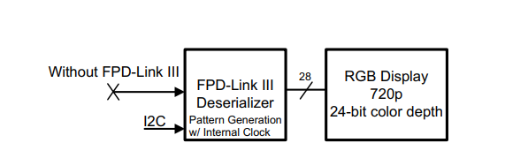
When using 948q1 (no serializer) test pattern , we were able to display the test screen normally on the screen, but the pixel clock is incorrect .
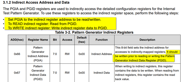
Internal Test Pattern Generation configuration mode
Desired pixel clock:2048 * 781 * 60 =95.96MHZ,we use Dual Link OpenLDI Output,so clk1 = clk2 = 47.98MHZ.
The configured internal clock:140MHZ / 3=46.66MHZ.
The actual measured pixel clock:CLK1 = CLK2 = 8MHZ.
Partial register configuration:
{0x66,0x03},
{0x66,0x03},
{0x63,0x01},
{0x64,0x41},
{0x65,0x04}.
Where is the problem?
好的。这里纠正一下上述错误的地方:间接寄存器0x03配置的值为0x03,对140MHZ内部时钟进行三分频。但是不管是二分频还是三分频,又或者其它分频,最终虽然都能出现测试图形,但是CLK1和CLK2输出的时钟都是在8MHZ左右,修改分频系数并不能改变像素时钟。
您好,应该是间接寄存器0x67 配置为0x03,设置为PCLK为140/3=46.66MHZ吧?
我看您这里是0x66 配置为0x03.0x67 的寄存器是PGID。
使用解串器ds90ub948q1的内部时钟,除了0x65寄存器,以及图形发生器间接地址中的图形发生器时钟分频器控制寄存器0x03之外,内部时钟分频还受什么影响呢?就948来说,在数据手册上我没有看到其它影响其内部时钟分频的寄存器。
您好,这几个寄存器的配置没问题。
我查了下资料,因为只使用948产生pattern的时候使用内部晶振是不稳定的,尤其是当分辨率不是常用分辨率时,内部晶振可能会导致不稳定,因此会出现这个问题,解决办法就是使用外部晶振去替代。
另外,如果配置dual link output的话,测试CLK1和CLK2的分辨率应该为PCLK的一半,比如,如果0x66配置为2的话,PCLK=70Mhz,那么CLK1=CLK2=35Mhz。
并且CLK1=CLK2=8MHz是默认值,也看起来0x66的值没有配置进去。
在配置0x66 分频系数的时候,您是否先配置,然后对其进行读,再去对0x66配置合适的分频系数这个步骤?