This thread has been locked.
If you have a related question, please click the "Ask a related question" button in the top right corner. The newly created question will be automatically linked to this question.
工具与软件:
您好、TI 专家:
我对 CBA9的诊断措施有疑问-无效事务的错误代码。 安全手册解释了这种诊断措施由硬件执行并会生成总线错误。 那么:
可以通过 R5FSS0_CORE0_INTR_IN_133中断来接收该诊断措施吗? 如果是、是否需要启用其他寄存器(例如 err_intr_enable_set)? 是否需要在中断回调中清除中断?
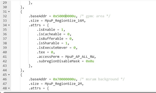
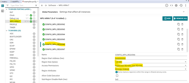
2.我需要测试这种诊断措施。 我是否可以直接将数据写入 PCIe 器件地址(0x69000000)以进行测试(在我的项目中、未使用 PCIe 器件且该器件尚未初始化)。 但是、在我的测试中、在尝试写入后、发生了数据中止异常。
测试日志:
数据中止:反向跟踪:
请使用:addr2line -e rtthread.elf -a -f ffffffff828e9a60[17103](带反向跟踪):回溯:未知符号地址 ffffffffffffffffff828e9a60
[17103] W/ backtrace: unred: index not founded ffffffff828e9a60.
执行:
R00:0x00000000 R01:0x69000000 R02:0xffffffff828e9a40 R03:0xffffffffffffffffffffff
r04:0xffffffffdeadbeh r05:0xffffffffdeadbeh r06:0xffffffffdeadbeh r07:0xffffffffdeadbeh
R08:0xffffffffdeadbeh R09:0xffffffffdeadbeh R10:0xffffffffdeadbeh
fp :0xffffffdeadbeef ip :0x00000000
SP :0xffffff84001948 LR :0x700b1798 PC :0xffffff828e9a68
CPSR:0x20000013
uint32_t ulTestData = 0U; void* hTransBufAddr = (void*)(CONFIG_PCIE0_OB_REG_L_TEST); memcpy(hTransBufAddr, &ulTestData, sizeof(uint32_t));
如果我的方法有问题、请给我一些指导。 我需要通过事件注入测试该诊断措施。
谢谢!
此致。
Kaijie
您好、Kaijie、
很抱歉,因为我昨天离开了,所以我的答复被推迟了。
您可能会在一天或两天内得到回复。
此致、
Anil。
您好、Kaijie、
[报价 userid="610902" url="~/support/microcontrollers/arm-based-microcontrollers-group/arm-based-microcontrollers/f/arm-based-microcontrollers-forum/1383212/am2432-the-handling-issues-of-diagnostic-measures-for-cba9---error-codes-for-invalid-transactions ]1. 是否可以通过 R5FSS0_CORE0_INTR_IN_133中断来接收该诊断措施? 如果是、是否需要启用其他寄存器(例如 err_intr_enable_set)? 是否需要在中断回调中清除中断?[/QUOT]我不确定 CBA9错误 是否会生成到 R5FSS0_CORE0_INTR_IN_133中断。
我可以将该主题转给正确的专家来评论您的问题。
但通常在 R5F 内核中、如果用户希望将中断路由到 R5F 内核、则需要启用中断、否则中断不会路由到 R5F 内核。
通常、启用 R5F 中断、我们执行以下步骤。
在清除中断时、已经有一个主 ISR、其中 MCU+SDK 将清除此中断。 因此、用户无需再次执行该操作。
此致、
Anil。
HwiP_Params hwiPrms; HwiP_Object cmpHwiObject; /* Register pin interrupt */ HwiP_Params_init(&hwiPrms); hwiPrms.intNum = ; hwiPrms.priority = //4U; hwiPrms.callback = //&IsrFxn; hwiPrms.isPulse = //TRUE; retVal = HwiP_construct(&cmpHwiObject, &hwiPrms); DebugP_assert(retVal == SystemP_SUCCESS );
模拟:
感谢您的答复。 请引导我联系另一位专家吗? 谢谢你。
Kaijie
尊敬的 凯杰:
您在使用哪个 SDK?
您能否分享详细信息、逐步在我们这边重现问题?
此致
Ashwani
尊敬的 Ashwani:
我要使用的 SDK 软件包为 mcu_plus_sdk_am243x_09_00_00_35。
实现过程:
必要条件:
1.启用 MPU、地址0x69000000UL 具有读写权限。
2. DPL 已初始化。
3.项目中没有 PCIe 设备、也没有任何设备已经初始化。
第1步:通过调用 DPL 接口、我注册并启用了 R5FSS0_CORE0_INTR_IN_133 (SDLR_R5FSS0_CORE0_INTR_GLOGIC_CBASS_INTR_OR_FORCE_MAIN_CBASS_AGG_ERR_INTR_0)。
第二步:尝试在地址0x69000000UL 处将数据写入 PCIe 器件。
执行写入时、系统进入数据中止中断、然后连续执行为 R5FSS0_CORE0_INTR_IN_133中断注册的回调函数。
如果我的测试方法存在问题、请指导我如何执行此诊断措施。
谢谢你。
Kaijie
感谢 Kaijie、
执行写入操作时、系统输入了数据中止中断、此后、系统连续执行为 R5FSS0_CORE0_INTR_IN_133中断注册的回调函数。
这不符合您的预期吗?
实施过程:
必要条件:
1.启用 MPU、地址0x69000000UL 具有读写权限。
2. DPL 已初始化。
3.项目中没有 PCIe 设备、也没有任何设备已经初始化。
第1步:通过调用 DPL 接口、我注册并启用了 R5FSS0_CORE0_INTR_IN_133 (SDLR_R5FSS0_CORE0_INTR_GLOGIC_CBASS_INTR_OR_FORCE_MAIN_CBASS_AGG_ERR_INTR_0)。
第2步:尝试在地址0x69000000UL 处将数据写入 PCIe 器件。[/QUOT]您对上述测试的预期是什么?
此致
Ashwani
你好、Ashwani。
感谢您的答复。
关于您的问题、我预计在执行 CBA9诊断过程测试后、只会调用注册的 R5FSS0_CORE0_INTR_IN_133中断回调函数来记录相关信息、而不会输入数据中止异常。 换句话说、CPU 需要继续正常运行。
参考:
如 TRM3.4节所述:"CBASS 检测到非法交易时、会缓慢地终止该交易、以避免系统挂起。 此外、CBASS 会将返回状态发送回初始方并显示错误状态。 如果该非法事务是读取事务、则读取数据返回全零。 如果该非法事务是写入事务、则该写入事务将被终止并向启动器返回写入错误。 可以在 CBASS 的 err_REGS 区域中找到中断和非法事务记录"
因此、我相信在执行测试后、只会生成一个错误报告、而不会影响 CPU 的正常运行。 如果我的理解不正确、请建议如何对 CBA9执行正确的测试。
此致
Kaijie
感谢 Kaijie、
MPU 已启用、且地址0x69000000UL 具有读写权限
您能否分享您为该区域所做的 SysConfig 和代码库的快照?
此致
Ashwani
我无法上传屏幕截图、但我可以提供代码片段。 在我们的工程中、我们尚未使用 SysConfig 工具进行配置。 以下是用于设置 MPU 的代码:
MpuP_RegionConfig gMpuRegionConfig[CONFIG_MPU_NUM_REGIONS + 4] = { { .baseAddr = 0x0u, /* back groud */ .size = MpuP_RegionSize_4G, .attrs = { .isEnable = 1, .isCacheable = 0, .isBufferable = 0, .isSharable = 1, .isExecuteNever = 0, .tex = 0, .accessPerm = MpuP_AP_S_RW, .subregionDisableMask = 0x0u }, }, { .baseAddr = 0x0u, /* vectors */ .size = MpuP_RegionSize_32K, .attrs = { .isEnable = 1, .isCacheable = 1, .isBufferable = 1, .isSharable = 0, .isExecuteNever = 0, .tex = 1, .accessPerm = MpuP_AP_S_R, .subregionDisableMask = 0x0u }, }, { .baseAddr = 0x50000000u, /* gpmc area */ .size = MpuP_RegionSize_16M, .attrs = { .isEnable = 1, .isCacheable = 0, .isBufferable = 0, .isSharable = 1, .isExecuteNever = 0, .tex = 0, .accessPerm = MpuP_AP_ALL_RW, .subregionDisableMask = 0x0u }, }, { .baseAddr = 0x70000000u, /* msram background */ .size = MpuP_RegionSize_2M, .attrs = { .isEnable = 1, .isCacheable = 1, .isBufferable = 1, .isSharable = 0, .isExecuteNever = 0, .tex = 1, .accessPerm = MpuP_AP_ALL_RW, .subregionDisableMask = 0x0u }, }, { .baseAddr = 0x80000000u, /* ddr background */ .size = MpuP_RegionSize_2G, .attrs = { .isEnable = 1, .isCacheable = 1, .isBufferable = 1, .isSharable = 0, .isExecuteNever = 0, .tex = 1, .accessPerm = MpuP_AP_ALL_RW, .subregionDisableMask = 0x0u }, }, { .baseAddr = 0x70080000u, /* kernel code */ .size = MpuP_RegionSize_512K, .attrs = { .isEnable = 1, .isCacheable = 1, .isBufferable = 1, .isSharable = 0, .isExecuteNever = 0, .tex = 1, .accessPerm = MpuP_AP_S_RW, .subregionDisableMask = 0x0u }, }, { .baseAddr = 0x70100000u, /* kernel data */ .size = MpuP_RegionSize_512K, .attrs = { .isEnable = 1, .isCacheable = 1, .isBufferable = 1, .isSharable = 0, .isExecuteNever = 0, .tex = 1, .accessPerm = MpuP_AP_S_RW, .subregionDisableMask = 0x0u }, }, { .baseAddr = 0x84000000u, /* memheap */ .size = MpuP_RegionSize_128M, .attrs = { .isEnable = 1, .isCacheable = 1, .isBufferable = 1, .isSharable = 0, .isExecuteNever = 0, .tex = 1, .accessPerm = MpuP_AP_ALL_RW, .subregionDisableMask = 0x0u }, }, { .baseAddr = 0x80000000u, /* rodata */ .size = MpuP_RegionSize_8M, .attrs = { .isEnable = 1, .isCacheable = 1, .isBufferable = 1, .isSharable = 0, .isExecuteNever = 0, .tex = 1, .accessPerm = MpuP_AP_ALL_R, .subregionDisableMask = 0x0u }, }, { .baseAddr = 0x80800000u, /* kernel bss */ .size = MpuP_RegionSize_8M, .attrs = { .isEnable = 1, .isCacheable = 1, .isBufferable = 1, .isSharable = 0, .isExecuteNever = 0, .tex = 1, .accessPerm = MpuP_AP_S_RW, .subregionDisableMask = 0x0u }, }, };
此外、我还使用提升的权限对其进行了测试。
谢谢、此致。
Kaijie
尊敬的 Kaijie:
从您的 SysConfig 来看、似乎 未启用存储器地址0x69000000UL。
以下是我的设置中包含的内容:
如果我缺少什么、请告诉我。
此致
Ashwani
嗨 Ashwani:
感谢您的指导。 这里确实有初始化问题、但在修改 MPU 初始化后、我尝试将数据写入地址0x69000000;但仍然遇到数据终止错误。
以下是我已经尝试过的修改后的 MPU 配置:
MpuP_RegionConfig gMpuRegionConfig[CONFIG_MPU_NUM_REGIONS + 4] = { { .baseAddr = 0x0u, /* back groud */ .size = MpuP_RegionSize_4G, .attrs = { .isEnable = 1, .isCacheable = 0, .isBufferable = 0, .isSharable = 1, .isExecuteNever = 0, .tex = 0, .accessPerm = MpuP_AP_S_RW, .subregionDisableMask = 0x0u }, }, { .baseAddr = 0x0u, /* vectors */ .size = MpuP_RegionSize_32K, .attrs = { .isEnable = 1, .isCacheable = 1, .isBufferable = 1, .isSharable = 0, .isExecuteNever = 0, .tex = 1, .accessPerm = MpuP_AP_S_R, .subregionDisableMask = 0x0u }, }, { .baseAddr = 0x50000000u, /* gpmc area */ .size = MpuP_RegionSize_16M, .attrs = { .isEnable = 1, .isCacheable = 0, .isBufferable = 0, .isSharable = 1, .isExecuteNever = 0, .tex = 0, .accessPerm = MpuP_AP_ALL_RW, .subregionDisableMask = 0x0u }, }, { .baseAddr = 0x68000000u, /* PCIE */ .size = MpuP_RegionSize_128M, .attrs = { .isEnable = 1, .isCacheable = 1, .isBufferable = 1, .isSharable = 1, .isExecuteNever = 0, .tex = 0, .accessPerm = MpuP_AP_ALL_RW, .subregionDisableMask = 0x0u }, }, { .baseAddr = 0x70000000u, /* msram background */ .size = MpuP_RegionSize_2M, .attrs = { .isEnable = 1, .isCacheable = 1, .isBufferable = 1, .isSharable = 0, .isExecuteNever = 0, .tex = 1, .accessPerm = MpuP_AP_ALL_RW, .subregionDisableMask = 0x0u }, }, { .baseAddr = 0x80000000u, /* ddr background */ .size = MpuP_RegionSize_2G, .attrs = { .isEnable = 1, .isCacheable = 1, .isBufferable = 1, .isSharable = 0, .isExecuteNever = 0, .tex = 1, .accessPerm = MpuP_AP_ALL_RW, .subregionDisableMask = 0x0u }, }, { .baseAddr = 0x70080000u, /* kernel code */ .size = MpuP_RegionSize_512K, .attrs = { .isEnable = 1, .isCacheable = 1, .isBufferable = 1, .isSharable = 0, .isExecuteNever = 0, .tex = 1, .accessPerm = MpuP_AP_S_RW, .subregionDisableMask = 0x0u }, }, { .baseAddr = 0x70100000u, /* kernel data */ .size = MpuP_RegionSize_512K, .attrs = { .isEnable = 1, .isCacheable = 1, .isBufferable = 1, .isSharable = 0, .isExecuteNever = 0, .tex = 1, .accessPerm = MpuP_AP_S_RW, .subregionDisableMask = 0x0u }, }, { .baseAddr = 0x84000000u, /* memheap */ .size = MpuP_RegionSize_128M, .attrs = { .isEnable = 1, .isCacheable = 1, .isBufferable = 1, .isSharable = 0, .isExecuteNever = 0, .tex = 1, .accessPerm = MpuP_AP_ALL_RW, .subregionDisableMask = 0x0u }, }, { .baseAddr = 0x80000000u, /* rodata */ .size = MpuP_RegionSize_8M, .attrs = { .isEnable = 1, .isCacheable = 1, .isBufferable = 1, .isSharable = 0, .isExecuteNever = 0, .tex = 1, .accessPerm = MpuP_AP_ALL_R, .subregionDisableMask = 0x0u }, }, { .baseAddr = 0x80800000u, /* kernel bss */ .size = MpuP_RegionSize_8M, .attrs = { .isEnable = 1, .isCacheable = 1, .isBufferable = 1, .isSharable = 0, .isExecuteNever = 0, .tex = 1, .accessPerm = MpuP_AP_S_RW, .subregionDisableMask = 0x0u }, }, };
MpuP_RegionConfig gMpuRegionConfig[CONFIG_MPU_NUM_REGIONS + 4] = { { .baseAddr = 0x0u, /* back groud */ .size = MpuP_RegionSize_4G, .attrs = { .isEnable = 1, .isCacheable = 0, .isBufferable = 0, .isSharable = 1, .isExecuteNever = 0, .tex = 0, .accessPerm = MpuP_AP_S_RW, .subregionDisableMask = 0x0u }, }, { .baseAddr = 0x0u, /* vectors */ .size = MpuP_RegionSize_32K, .attrs = { .isEnable = 1, .isCacheable = 1, .isBufferable = 1, .isSharable = 0, .isExecuteNever = 0, .tex = 1, .accessPerm = MpuP_AP_S_R, .subregionDisableMask = 0x0u }, }, { .baseAddr = 0x50000000u, /* gpmc area */ .size = MpuP_RegionSize_16M, .attrs = { .isEnable = 1, .isCacheable = 0, .isBufferable = 0, .isSharable = 1, .isExecuteNever = 0, .tex = 0, .accessPerm = MpuP_AP_ALL_RW, .subregionDisableMask = 0x0u }, }, { .baseAddr = 0x68000000u, /* PCIE */ .size = MpuP_RegionSize_128M, .attrs = { .isEnable = 1, .isCacheable = 0, .isBufferable = 0, .isSharable = 1, .isExecuteNever = 0, .tex = 0, .accessPerm = MpuP_AP_ALL_RW, .subregionDisableMask = 0x0u }, }, { .baseAddr = 0x70000000u, /* msram background */ .size = MpuP_RegionSize_2M, .attrs = { .isEnable = 1, .isCacheable = 1, .isBufferable = 1, .isSharable = 0, .isExecuteNever = 0, .tex = 1, .accessPerm = MpuP_AP_ALL_RW, .subregionDisableMask = 0x0u }, }, { .baseAddr = 0x80000000u, /* ddr background */ .size = MpuP_RegionSize_2G, .attrs = { .isEnable = 1, .isCacheable = 1, .isBufferable = 1, .isSharable = 0, .isExecuteNever = 0, .tex = 1, .accessPerm = MpuP_AP_ALL_RW, .subregionDisableMask = 0x0u }, }, { .baseAddr = 0x70080000u, /* kernel code */ .size = MpuP_RegionSize_512K, .attrs = { .isEnable = 1, .isCacheable = 1, .isBufferable = 1, .isSharable = 0, .isExecuteNever = 0, .tex = 1, .accessPerm = MpuP_AP_S_RW, .subregionDisableMask = 0x0u }, }, { .baseAddr = 0x70100000u, /* kernel data */ .size = MpuP_RegionSize_512K, .attrs = { .isEnable = 1, .isCacheable = 1, .isBufferable = 1, .isSharable = 0, .isExecuteNever = 0, .tex = 1, .accessPerm = MpuP_AP_S_RW, .subregionDisableMask = 0x0u }, }, { .baseAddr = 0x84000000u, /* memheap */ .size = MpuP_RegionSize_128M, .attrs = { .isEnable = 1, .isCacheable = 1, .isBufferable = 1, .isSharable = 0, .isExecuteNever = 0, .tex = 1, .accessPerm = MpuP_AP_ALL_RW, .subregionDisableMask = 0x0u }, }, { .baseAddr = 0x80000000u, /* rodata */ .size = MpuP_RegionSize_8M, .attrs = { .isEnable = 1, .isCacheable = 1, .isBufferable = 1, .isSharable = 0, .isExecuteNever = 0, .tex = 1, .accessPerm = MpuP_AP_ALL_R, .subregionDisableMask = 0x0u }, }, { .baseAddr = 0x80800000u, /* kernel bss */ .size = MpuP_RegionSize_8M, .attrs = { .isEnable = 1, .isCacheable = 1, .isBufferable = 1, .isSharable = 0, .isExecuteNever = 0, .tex = 1, .accessPerm = MpuP_AP_S_RW, .subregionDisableMask = 0x0u }, }, };
Kaijie
您好、专家。
您是否有关于此问题的任何更新?
谢谢你
此致
Kaijie