请注意,本文内容源自机器翻译,可能存在语法或其它翻译错误,仅供参考。如需获取准确内容,请参阅链接中的英语原文或自行翻译。
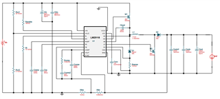
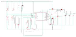
器件型号:LM25118 我有另一个基于此设计的设计、因此我知道所使用的组件会起作用。 我最初制作的设计与 webench 生成的设计类似:
输入为10-24V、最大电流为7A
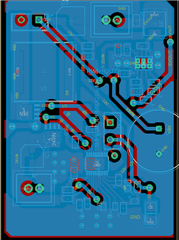
在我确认可以正常工作后、我制作了一个更小版本的电路板、以便将它与另一个电路板结合使用。 新电路板将无法正常工作。 首次打开时、输出电压为11.8、但施加负载后、电压开始随较大负载线性下降。 关闭并重新打开后、电压不会恢复正常。 我用2种不同的芯片尝试过它。 我不知道我是否把它们烧掉了,但它们变得很热。 有2页我合并到一个板上,但第二是无关紧要,就我知道。
顶部:
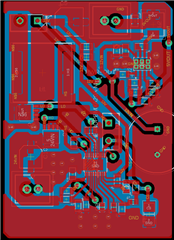
顶部:
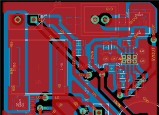
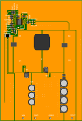
底部:
底部: