This thread has been locked.

If you have a related question, please click the "Ask a related question" button in the top right corner. The newly created question will be automatically linked to this question.

TMS320F28377D: TI的工程师你们好,28377D双核通信存在一个问题,具体问题如下:

Part Number: TMS320F28377D


DSP双核IPC通信,CPU1同样一个数组readData,我把他放在MSGRAM_CPU1_TO_CPU2里面,传输给CPU2,CPU2读取到的readData地址正确,但是我把数组readData放在RAMGS0中,CPU2读取到的readData地址错误,本来地址应该是0x00C000,现在是0x8000C000,这是为什么呢?我CPU1和CPU2的CMD文件都定义了RAMGS0的起始位置和长度,RAMGS0由CPU1控制。

此外我还有一个问题,就是我在CPU1和CPU2都定义了GSRAM0的话,他们是共享这一片GSRAM0还是说CPU1有一块GSRAM0,CPU2有另外的GSRAM0呢?

  • CPU1代码如下

    //
    // Included Files
    //
    #include "driverlib.h"
    #include "device.h"
    #include "board.h"
    #include "F2837xD_device.h"     // F2837xD Headerfile Include File
    //
    // Defines
    //
    #define IPC_CMD_READ_MEM   0x1001
    #define IPC_CMD_RESP       0x2001
    
    #define TEST_PASS          0x5555
    #define TEST_FAIL          0xAAAA
    
    
    #pragma DATA_SECTION(readData, "readDataRAM")
    uint32_t readData[10];
    uint16_t IPCpass;
    uint32_t pass;
    
    IPC_MessageQueue_t messageQueue;
    IPC_Message_t      TxMsg, RxMsg;
    //
    // Main
    //
    void main(void)
     {
        int i;
    
        //
        // Initialize device clock and peripherals
        //
        Device_init();
    
        //
        // Initialize PIE and clear PIE registers. Disables CPU interrupts.
        //
        Interrupt_initModule();
    
        //
        // Initialize the PIE vector table with pointers to the shell Interrupt
        // Service Routines (ISR).
        //
        Interrupt_initVectorTable();
    
        //
        // Initialize settings from SysConfig
        //
        Board_init();
    
        //
        // Give Memory Access to GS0/ GS14 SARAM to CPU02
        //必须在CPU2启动前分配
    //        while( !(MemCfgRegs.GSxMSEL.bit.MSEL_GS0 &
    //                 MemCfgRegs.GSxMSEL.bit.MSEL_GS14))
        while( !(MemCfgRegs.GSxMSEL.bit.MSEL_GS14))//GS14未分配给CPU02则循环
            {
                EALLOW;
                MemCfgRegs.GSxMSEL.bit.MSEL_GS0 = 0;// 将 GS0 分配给 CPU01
                MemCfgRegs.GSxMSEL.bit.MSEL_GS14 = 1;// 将 GS14 分配给 CPU02
                EDIS;
            }
        //
        // Give memory access to GS0 and GS14 RAM to CPU2
        // driverlib库开发写法
    //    MemCfg_setGSRAMMasterSel((MEMCFG_SECT_GS0 | MEMCFG_SECT_GS14),
    //                             MEMCFG_GSRAMMASTER_CPU2);
    //    MemCfg_setGSRAMMasterSel((MEMCFG_SECT_GS14),
    //                             MEMCFG_GSRAMMASTER_CPU2);
    
        //
        // Initialize GPIO and configure the GPIO pin as a push-pull output
        //
        Device_initGPIO();
    
        GPIO_setPadConfig(99, GPIO_PIN_TYPE_STD);
        GPIO_setDirectionMode(99, GPIO_DIR_MODE_OUT);
        GPIO_setMasterCore(99, GPIO_CORE_CPU1);
    
        GPIO_setPadConfig(133, GPIO_PIN_TYPE_STD);
        GPIO_setDirectionMode(133, GPIO_DIR_MODE_OUT);
        GPIO_setMasterCore(133, GPIO_CORE_CPU2);
    
    
        //
        // Clear any IPC flags if set already
        //
        IPC_clearFlagLtoR(IPC_CPU1_L_CPU2_R, IPC_FLAG_ALL);
    
        //
        // Initialize message queue
        //
        IPC_initMessageQueue(IPC_CPU1_L_CPU2_R, &messageQueue, IPC_INT1, IPC_INT1);
    
        //
        // Synchronize both the cores
        //
        IPC_sync(IPC_CPU1_L_CPU2_R, SYNC_FLAG);


        //
        // Enable Global Interrupt (INTM) and realtime interrupt (DBGM)
        //
        EINT;
        ERTM;
    
        //
        // Fill in the data to be sent
        //
        for(i=0; i<10; i++)
        {
            readData[i] = i;
        }
    
        //
        // Update the message
        //
        TxMsg.command = IPC_CMD_READ_MEM;
        TxMsg.address = (uint32_t)readData;
    //    TxMsg.address = (uint32_t)readData;
        TxMsg.dataw1  = 10;  // Using dataw1 as data length
        TxMsg.dataw2  = 1;   // Message identifier
    
    
        //
        // End of example. Loop forever
        //
        while(1)
        {
            DEVICE_DELAY_US(1000000);
    //        GPIO_togglePin(133);
            GPIO_togglePin(99);
            IPC_sendMessageToQueue(IPC_CPU1_L_CPU2_R, &messageQueue, IPC_ADDR_CORRECTION_ENABLE,
                                   &TxMsg, IPC_BLOCKING_CALL);
    
            IPC_readMessageFromQueue(IPC_CPU1_L_CPU2_R, &messageQueue, IPC_ADDR_CORRECTION_DISABLE,
                                     &RxMsg, IPC_BLOCKING_CALL);
    
            if((RxMsg.command == IPC_CMD_RESP) && (RxMsg.dataw1 == TEST_PASS) && (RxMsg.dataw2 == 1))
            {
                pass = 1;
                IPCpass++;
            }
            else
                pass = 0;
        }
    }


  • CPU2代码如下

    #include "driverlib.h"
    #include "device.h"
    #include "board.h"
    #include "F2837xD_device.h"     // F2837xD Headerfile Include File
    
    //
    // Defines
    //
    #define IPC_CMD_READ_MEM   0x1001
    #define IPC_CMD_RESP       0x2001
    
    #define TEST_PASS          0x5555
    #define TEST_FAIL          0xAAAA
    
    #define GS0_Start          0x00C000
    #define ARRAY_LENGTH 10  // 假设数组长度为 10
    
    IPC_MessageQueue_t messageQueue;
    IPC_Message_t TxMsg, RxMsg;
    uint16_t IPCCount;
    uint32_t command, addr, data;
    bool status = false;
    uint32_t readData2[10];
    #pragma DATA_SECTION(readData2, "readData2")


    //
    // Function prototypes
    //
    __interrupt void IPC_1_ISR(void);
    
    //
    // Main
    //
    void main(void)
    {
        int j=0;
        //
        // Initialize device clock and peripherals
        //
        Device_init();
    
        //
        // Initialize PIE and clear PIE registers. Disables CPU interrupts.
        //
        Interrupt_initModule();
    
        //
        // Initialize the PIE vector table with pointers to the shell Interrupt
        // Service Routines (ISR).
        //
        Interrupt_initVectorTable();
    
        Board_init();
    
        //
        // Clear any IPC flags if set already
        //
        IPC_clearFlagLtoR(IPC_CPU2_L_CPU1_R, IPC_FLAG_ALL);
    
        //
        // Initialize message queue
        //
        IPC_initMessageQueue(IPC_CPU2_L_CPU1_R, &messageQueue, IPC_INT1, IPC_INT1);
    
        //
        // Enable Global Interrupt (INTM) and realtime interrupt (DBGM)
        //
        EINT;
        ERTM;
    
        //
        // Synchronize both the cores.
        //
        IPC_sync(IPC_CPU2_L_CPU1_R, SYNC_FLAG);
    
    
        while(1);
    }
    
    //
    // IPC ISR for Flag 1
    // C28x core sends data with message queue using Flag 0
    //
    __interrupt void IPC_1_ISR(void)
    {
        int i,j;
    //    IPC_Message_t TxMsg, RxMsg;
    //    bool status = false;
        IPCCount++;
    
        //利用GS0基地址读取
        for(j=0; j<ARRAY_LENGTH; j++)
           {
                readData2[j]=*((uint32_t *)GS0_Start+j);
           }
    
        //
        // Read the message from the message queue
        //
        IPC_readMessageFromQueue(IPC_CPU2_L_CPU1_R, &messageQueue, IPC_ADDR_CORRECTION_ENABLE,
                                 &RxMsg, IPC_NONBLOCKING_CALL);
    
    
        if(RxMsg.command == IPC_CMD_READ_MEM)
        {
            status = true;
    
            //
            // Read and compare data
            //
            for(i=0; i<RxMsg.dataw1; i++)
            {
                if(*((uint32_t *)RxMsg.address + i) != i)
                    status = false;
            }
        }
    
        //
        // Send response message
        //
        TxMsg.command = IPC_CMD_RESP;
        TxMsg.address = 0; // Not used
        TxMsg.dataw1  = status ? TEST_PASS : TEST_FAIL;
        TxMsg.dataw2  = RxMsg.dataw2; // Use the message identifier from the received message
    
        IPC_sendMessageToQueue(IPC_CPU2_L_CPU1_R, &messageQueue, IPC_ADDR_CORRECTION_DISABLE,
                               &TxMsg, IPC_NONBLOCKING_CALL);
    
        DEVICE_DELAY_US(1000000);
        GPIO_togglePin(133);
    
    //    uint32_t command, addr, data;
    //    bool status = false;


        //
        // Acknowledge the flag
        //
        IPC_ackFlagRtoL(IPC_CPU2_L_CPU1_R, IPC_FLAG1);
    
        //
        // Acknowledge the PIE interrupt.
        //
        Interrupt_clearACKGroup(INTERRUPT_ACK_GROUP1);
    }
    
    //
    // End of File
    //
    

  • 我不传递数组,仅仅只是传递一个宏定义,定义的是数组的首地址,为什么也是不行呢,地址还是会变为0x8000C000

  • 另外,DSP可以把GSRAM在CMD里面修改分配给MSGRAM_CPU1_TO_CPU2吗,这样的话也能解决问题

  • 又出现了一个问题:数组readData,我把他放 
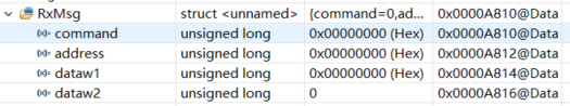
在MSGRAM_CPU1_TO_CPU2里面,传输给CPU2,若是传输的数组大一点例如uint32_t readData[70];,,CPU2的RxMsg都为0了。这是为什么呢??

  • 已经收到了您的案例,调查需要些时间,感谢您的耐心等待。

  • 您好

    CPU1和 CPU2在物理上没有不同的 GSRAM0、它是相同的存储器。 根据 GSxMSEL 寄存器的配置、任一 CPU 拥有该寄存器。 您是否还可以说明将此部分"readData2"映射到了哪个存储器? 在您共享的代码中、在 CPU2中、您对 GS0_Start 进行硬编码并直接读取 readData2[]。 我希望这可以正常工作。 运行代码时、我观察到 CPU1将地址0xC000放入消息队列(不考虑 IPC_sendMessageToQueue 中设置的 addrCorrEnable 参数)、当 CPU2读取队列时、它会转换地址。 既然我们使用的是 GSRAM、您可以尝试使用 IPC_ADDR_CORRECTION_DISABLE 吗?

  • readData2我放在了RAMGS14,我设置RAMGS14的主核是CPU2,可以对其读写。在CPU1我把数组放在RAMGS0中,我把RAMGS0的起始地址定义为GS0_Start ,在CPU2中直接用GS0_Start 读取数据是没有问题的。意思就是如果我在CPU1中把数组放在GSRAM而不是MSGRAM的话,不用地址校正就可以吗?我去尝试一下。另外这个地址校正是什么意思我还没弄明白,为什么会需要地址校正呢?相关的资料在哪里查呢?

  • 非常感谢,刚刚我尝试了一下使用GSRAM的话采用IPC_ADDR_CORRECTION_DISABLE,现在地址就正确了,为什么用GSRAM就不用地址校正,用MSGRAM就需要呢?麻烦你再给我解释一下。

  • 是的,对于GSRAM来说采用IPC_ADDR_CORRECTION_DISABLE 就可行了,但是为什么利用MSGRAM的时候需要IPC_ADDR_CORRECTION_ENABLE呢?可以为我解答一下吗?

  • 您好

    感谢您的回复!

    如果相关建议已经解决您问题,将关闭本贴,如果您还有问题,请再次发帖,十分感谢。

  • 还有一个疑问呀。为什么数组存放在GSRAM采用IPC_ADDR_CORRECTION_DISABLE,存放在MSGRAM的时候需要IPC_ADDR_CORRECTION_ENABLE呢?只有这一个疑问了。

  • 您好

    应在 sendMessage 和 readMessage 函数调用中禁用地址校正(IPC_ADDR_CORRECTION_DISABLE)。

  • 这个我知道,请仔细看我的问题,我是询问的为什么GSRAM不需要校正,而MSGRAM需要校正。

  • 您好

    这是因为 API 实现假定使用 MSGRAM。 如果启用了地址校正、它会将地址发送到 MSGRAM 基址。 当您将其与 GSRAM 一同使用时、地址将损坏。

  • 我的理解是因为GSRAM对于CPU1和CPU2是一个地址,但是MSGRAM具有指向性,若是CPU1TOCPU2RAM,是否可以认为同一块区域在CPU1和CPU2的地址不一样呢?

  • 您好

    是的、GSRAM 地址同时适用于 CPU1和 CPU2。 CPU1TOCPU2RAM 在 CPU1和 CPU2中也是相同的地址、没有什么不同、只是访问权限不同。 MSGRAM 具有来自其自身 CPU 子系统的 CPU/DMA 读取/写入访问权限、以及来自其他子系统的 CPU/DMA 只读权限。