Part Number: TMS320F28035
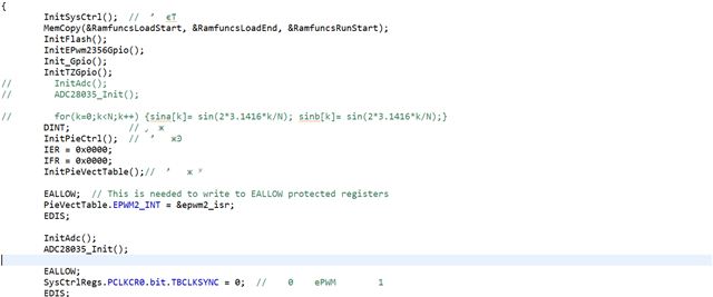
在使用EPwm中断的程序中,我将ADC初始化InitAdc()函数放在EPWM模块的TBCLK(时基时钟)关闭和开启前,AdcResult全为0,如果放在TBCLK(时基时钟)关闭和开启后,AdcResult就有值。
想请问下这是什么问题。
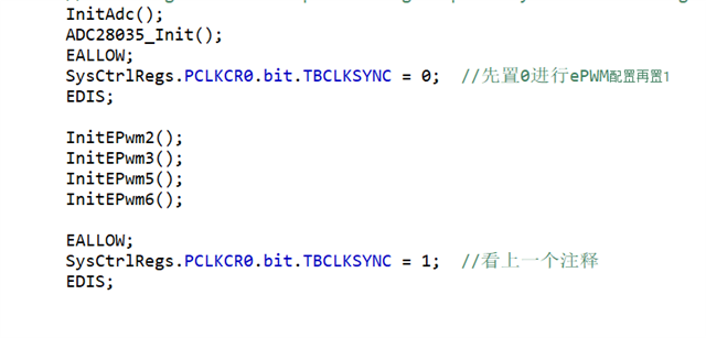
Part Number: TMS320F28035
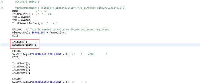
在使用EPwm中断的程序中,我将ADC初始化InitAdc()函数放在EPWM模块的TBCLK(时基时钟)关闭和开启前,AdcResult全为0,如果放在TBCLK(时基时钟)关闭和开启后,AdcResult就有值。
想请问下这是什么问题。