Part Number: TMS320F28035
Other Parts Discussed in Thread: C2000WARE, CONTROLSUITE
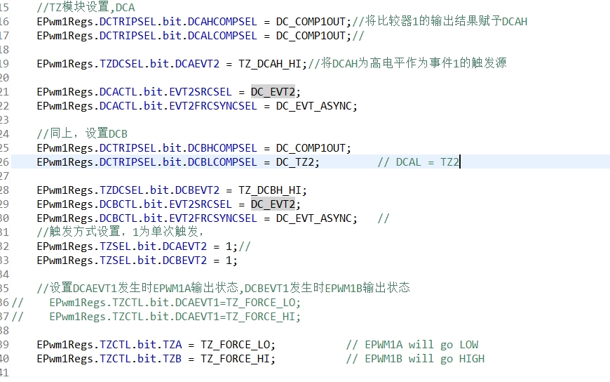
按照如图设置了epwm1的DC以及TZ模块,当COMP1OUT输出高电平时,EPWM1A输出低电平,EPWM1B输出高电平,但是现在COMP1OUT有输出了,但是EPWM1输出并未发生变化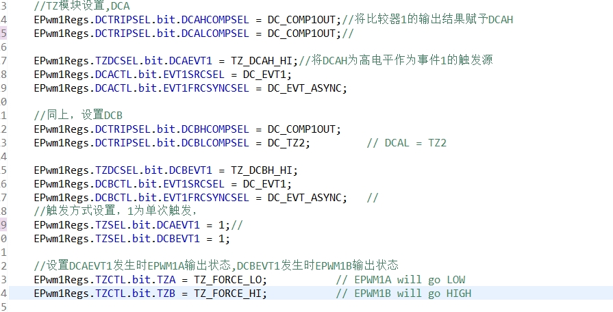
Part Number: TMS320F28035
Other Parts Discussed in Thread: C2000WARE, CONTROLSUITE
按照如图设置了epwm1的DC以及TZ模块,当COMP1OUT输出高电平时,EPWM1A输出低电平,EPWM1B输出高电平,但是现在COMP1OUT有输出了,但是EPWM1输出并未发生变化

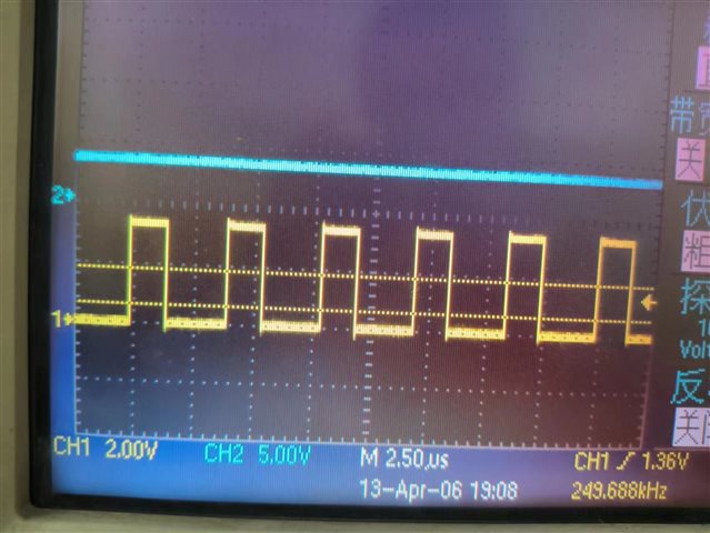

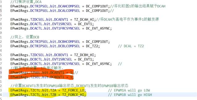
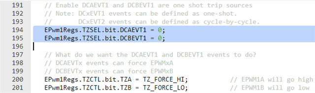
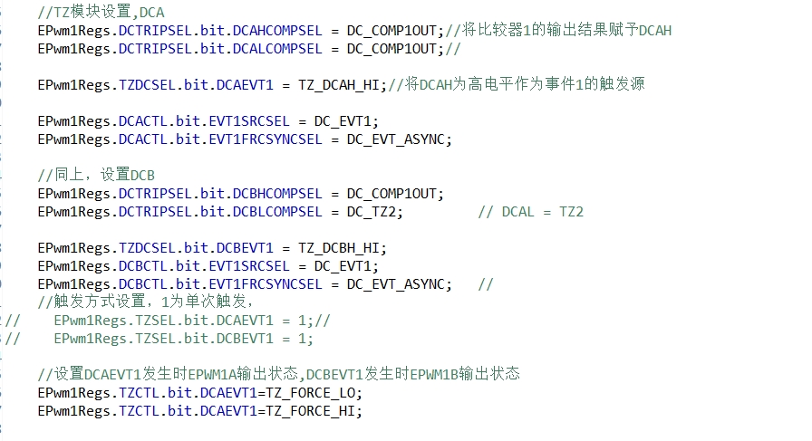 您好,按照您说方法尝试了一下,EPWM1的输出还是没有任何变化,两种方法尝试代码如图
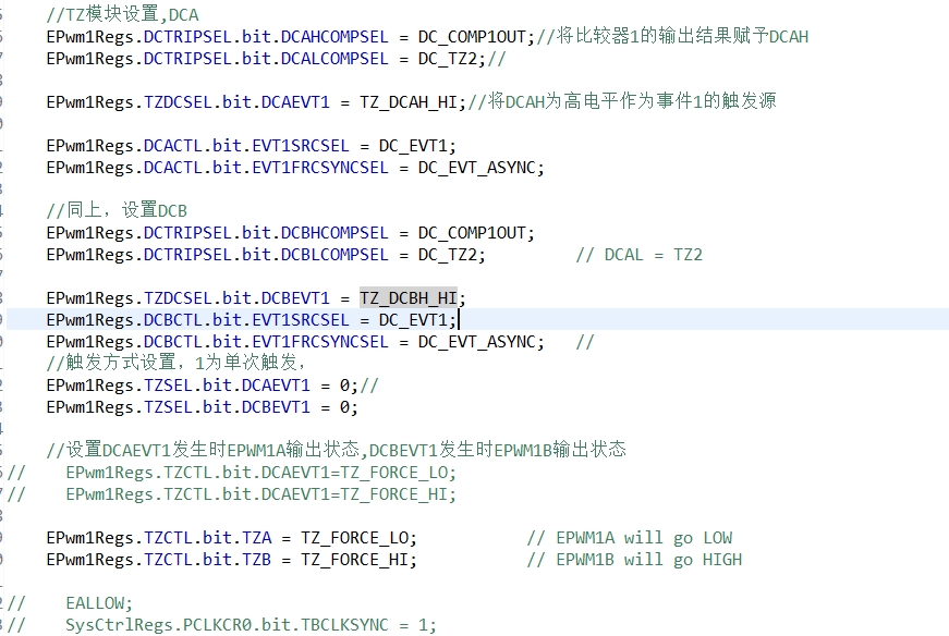 这是EPWM1的配置